This thread has been locked.

If you have a related question, please click the "Ask a related question" button in the top right corner. The newly created question will be automatically linked to this question.

LM5148: LM5148

Part Number: LM5148

Hello 

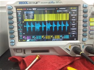
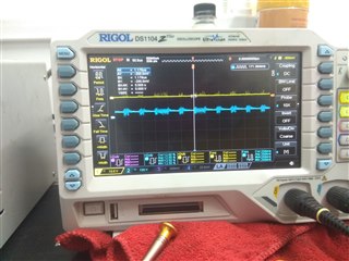
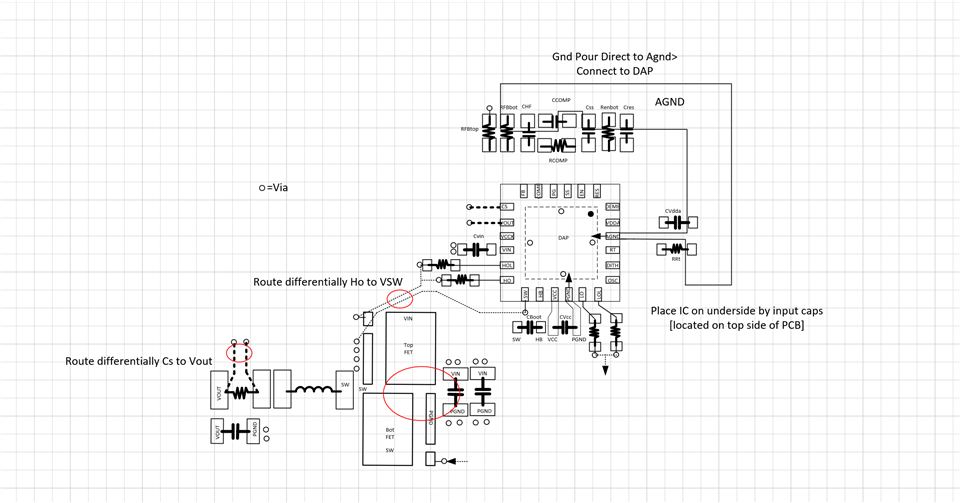
I have implemented modifications to my PCB board based on discussions in the TI forum. Nevertheless, the MOSFET is encountering damage on both the high and low sides, and the PWM waveform continues to be ungenerated. I have attached a photo of the PWM waveform for your review. I am seeking recommendations for appropriate MOSFETs for my design, in case my current MOSFET selection is incorrect. Additionally, I would appreciate insights on generating PWM without utilizing both MOSFETs or How can PWM will generate with MOSFETs. Furthermore, there is a discrepancy in the output voltage, as it is producing 8.5 volts instead of the intended 12V.


  • Hello Sanjana,

    Can you link the previous E2E so I can review history.  If you have not done so already, please fill out the design calculator.

    0511.LM5148-LM25148 Quickstart Calculator dsb edits.xlsm

    Thanks.

    David.

  • I've included the link to our previous E2E discussion. I am attaching my schematic, PCB layout and design calculator. Please take a look at the conversation history and advise on how to address the issues in my DC to DC converter. Additionally, could you recommend any Texas Instruments support in India that I can reach out to for technical assistance with my project?

    link of previous discussion on E2E forum:  https://e2e.ti.com/support/power-management-group/power-management/f/power-management-forum/1302936/lm5148-power-management-forum

    RM-004-V-01.PcbDocRM-004-V-00 calculator.xlsm

    RM-004-V-01.SchDoc

  • Please respond promptly with solutions to the aforementioned issues. I am eagerly awaiting your guidance.

  • Hello Sanjana,

    Part of the problem is you are laying this out on a two-layer board, so you don't have a solid ground plane.  As such the distances you have are creating undesirable parasitic inductances.   you output ground connection does not need to be connected to a low inductance path to input ground.  however, the input cap ground needs a low inductance path to the source of the low side MOSFET and the Input cap +ve needs to be connected with a low inductance path to the drain of the HS mosfet..  the loop formed by these components need to be tight.  it's not so much the width of the copper but the loop you are forming that is proportional to the parasitic inductance, as such this layout is not good.  Hence the issues you are having.  Ideally you will want a solid ground plane directly beneath the power stage on the top forming a tight loop, but it's impossible to achieve that here.  so, you will need to layout it out a little differently.  suggest you start with the concept shown below.  different device same concept.  also having two top FETs and two bottom FET further complicates things, perhaps you could get away with a single top and bottom FET?

    Hope this helps.

    David.