This thread has been locked.

If you have a related question, please click the "Ask a related question" button in the top right corner. The newly created question will be automatically linked to this question.

TPS546D24A: Noisy VR, need to verify design and hw/sw configuration

Part Number: TPS546D24A

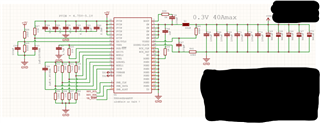
Our recent design has the main VR: TPS546D24ARVF, Vin=5V, Vout=0.295V,nom at 40A Imax.

Problem statement:

The VR is very noisy and leaking noise into clocks.

High level request:

The power design is straightforward and shouldn't have these issues. We implemented the design in WeBench and followed the design recommendations 100%. So before I look into design improvements, e.g. layout, I want to verify basic hw/sw configuration. (Sometimes it is one silly mistake or error that causes everything to not work!)

Specific requests:

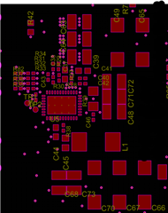
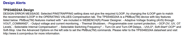
(1) Check for errors in WeBench recommendation, including passive values, resistor strap settings, etc. I uploaded the WeBench pdf.

(2) Configuration file vs. defaults? We had difficulty connecting through the TI Fusion GPIO/I2C dongle, so we have been using a Raspberry Pi for basic configuration through I2C. Our current methodology assumes the configuration defaults are "healthy" given the proper resistor strappings (e.g. MSEL,VSEL,ADRSEL). For example, the default frequency is 550 kHz (read from I2C), and this matches WeBench, so the default is OK. One of my concerns is there could be settings made when providing a config file with Fusion that we are not supplying since we are using the RPi, whether they are "hidden" settings or we are just missing them on our end.

(3) Noise leakage is occurring onto a UART Clock at ~3MHz, and a PLL Refclk at 20-40MHz.

I haven't done deep qualitative analysis on the noise, but it shows up in a scope capture of the clock (550kHz), and the UART is non-functional with the VR switching (even under light loads). Our workaround to get the board running is with an external EVM (we have systems working with the TPS546D24A and the TPS546B24A-2PH).

Thanks in advance for your help!

  • WBDesign5V-40A.pdf

    It appears my initial upload attempt failed. Here is the WeBench we used for this design.

  • Hi Tom,

    Often times noise issues can be caused by non ideal layout. Can you share the layout of the TPS546D24A?

    How are you measuring the noise? Does your scope probe have a long GND lead that could be picking up the switching noise? 

    What is supplying the 5V input and how far away is it supplied? You might consider increasing the input capacitance by another 1-2x47uF to reduce VIN ripple.

    Thanks,

    Joseph

  • Hi

    Thanks for your response, although you didn't answer my questions about the WeBench circuit or the configuration file, (1) or (2) above. Can you please try and address these?

    I cannot share the full design since this is a public forum, although the input and output power stages are quite standard. Here are some screenshots showing the basic design. Again, we followed WeBench for the schematic.

    How am I measuring the noise? I'm using a Siglent oscilloscope on the SE clock line, with a GND probe attached from the probe to a nearby GND location. It's the best we can do on the current setup. Yes, admittedly I have picked up some switching noise while probing, and I can see the noise amplitude vary depending on how I hold the probe and which GND point I select. Nevertheless, I'm confident there is still noise leaking into the clock signals without probe interference, since my clocks are not well (e.g. UART nonfunctional) while using the on-board TPS, but as soon as I use an external TPS-EVM to source the VDD rail, the UART is functional.

    5V input is from a banana connector less than 1.5" away (the entire board is under 6" square).

    Thanks,

    Tom

    PS - we will be building a new version of this board and I greatly rely on some TI input for this board to be successful. If E2E is not sufficient to address my concerns, let's please try and arrange another support method. Much appreciated.

  • Hi Tom,

    Joseph will reply you after New Year Holiday.

  • On further review, I just noticed this message in the WeBench regarding a "Design Error Message" - "Selected PINSTRAPPING setting does not give the required ILOOP."

    Please confirm whether this is relevant to our current issue, and if so, how to resolve.

    Thanks,

    Tom

  • Hi Tom,

    In regards to your original questions:

    1) Because your design uses 0.3Vout, the only way to configure this is through PMBus once the device has powered on (you can't select 0.3V through pinstrapping). Webench is recommending values assuming that you are configuring the device mostly with PMBus (Using the Fusion GUI or command line tools). So, it seems that the pinstrapped values that Webench is recommending are giving you the incorrect settings.

    The resistors used for MSEL1 select 325kHz FSW and COMP# 5, which isn't what you are expecting.

    The device default is to use pinstrapping, so on the initial bootup it will use the pinstrapped configuration. After the first bootup you can disable pinstrapping as needed for the different parameters to get the desired configuration, in which you are able to store values into the NVM of the device and use them instead of the pinstrapped values.

    The datasheet specifies a register called PIN_DETECT_OVERRIDE which allows you to select pinstrap vs. NVM stored value for the main parameters selected by VSEL, MSEL1, MSEL2, and ADRSEL. 

    Once you set all the values and configuration using PMBus, you have to make sure to store to NVM so that the device will hold the changes made after a power cycle. This way the device will boot up with your desired configuration.

    I'm happy to setup a call to walk through this configuration with you if it is easier.

    Thanks,

    Joseph

  • Hi, Joseph,

    Thanks for your reply.

    We are aware of the requirement to use PMBUS, as the default Vout (with the pinstrap settings configured per Webench) is ~1.2V. After configuring, we are getting the desired Vout of 300mV. And we can read/write the voltage/FSW as desired through PMBUS. This is confirmed on both the on-board VR and the EVM using the same RPi as the PMBUS host.

    Side question: if we change the voltage and/or the FSW through PMBUS, are all of the tuning parameters (i.e. compensation values) automatically changed as needed? This is critical for us to get right, as we chose this VR to be able to change and tune Vout dynamically. My high-level assumption is that if we tell the VR to change voltage and it complies, it should "know" the accompanying compensation values and tune itself, thus handling the minutiae to optimize regulation.

    I am checking with my firmware engineer what configuration values he currently sends from the RPi. Meanwhile, can you advise the correct values we should be sending through PMBUS for our application? I will try the spreadsheet tool again but find it a little confusing. (for clarity, this is the spreadsheet I'm using: www.ti.com/.../SLUC686)

    Lastly, some feedback... If I understand your response correctly, you are confirming that the WeBench recommendation is not valid for our application with Vout of 300mV. The recommendation includes the "Operating Values" table, and some of these values are incorrect (e.g. line 25. CPI 32.0 pF may not be correct). Again, I don't know what values we input but I think our fw engineer followed WeBench. So the feedback is simply this: WeBench should give the correct and full recommendation to match the capability of the VR. If the range of the VR goes down to 300mV, why doesn't the tool accomodate this? Even worse, it is giving faulty information! To summarize, there is an error in the WeBench recommendation related to pinstraps (hardware resistors) and the PMBUS operating values. I'm still waiting for TI to confirm that the rest of the WeBench recommendation is correct.


    Thanks,

    Tom

  • Hi Tom,

    The spreadsheet you'll want to use is here: SLURB01 Calculation tool | TI.com

    Compensation values are not automatically tuned to the correct value for the output voltage. This is what the design calculator I linked is for. I can help guide you through the compensation selection process. 

    Can you start by filling in the calculator with your key design parameters (should be the first sheet/page and the one with pinstrapping)?

    The incorrect pinstrapping values are a bug in the WEBENCH Model that I will work request to have fixed.

    Thanks,

    Joseph

  • Hi Tom,

    I reviewed the rest of the WEBENCH design and it looks like the only affected item is the MSEL1 resistors. Besides VSEL selecting 1.2V (which you would have to change through PMBus anyways), MSEL2 is correct (standalone device) and ADRSEL is correctly selecting address 36d.

    The main parameters you should change through PMBus then are FSW (change to 550kHz (and store into NVM)) and compensation. For compensation we will need to use the SLURB01 design calculator I link above (fill it out and return to me), then we can program the compensation correctly.

    The big issue I see on the layout is that pretty much all power components use a thermal relief connect style on VIN, PGND, and VOUT planes. This is not recommended because it greatly increases the amount of parasitics in the board (ESL and ESR), which is likely contributing to the high frequency noise you are seeing and impact the performance. 

    Another thing for noise you can check is the SW node, using a tip and barrel measurement method with your scope probe. I am expecting there could be some excess ringing on the SW node at those target frequencies you mentioned ~30MHz.

    Let me know when you have filled out the calculator spreadsheet.

    Thanks,

    Joseph

  • SLURB01-TPS546D24A_2024-01-04.xlsx

    Hi Joseph,

    The TPS webpage is a little confusing, then, regarding which spreadsheet to use. https://www.ti.com/product/TPS546D24A?utm_source=google&utm_medium=cpc&utm_campaign=app-bsr-null-44700045336317446_prodfolderdynamic-cpc-pf-google-wwe_int&utm_content=prodfolddynamic&ds_k=DYNAMIC+SEARCH+ADS&DCM=yes&gad_source=1&gclid=Cj0KCQiAy9msBhD0ARIsANbk0A8gV5zx9V9Z17TO9mnHg_pRTuLx76UxwVdo8shvC2LUkPpPstI_65saAvfXEALw_wcB&gclsrc=aw.ds#design-tools-simulation
    SLUC686 is "Compensation and Pin-Strap Resistor Calculator", which sounds like the right calculator to use for compensation...but anyways, thanks for clarifying!

    Here is the SLURB01. I filled it out as best I could with our basic design parameters and some values from Webench.

    RE: thermal relief on the layout--noted, and we will do a solid pour for the next PCB revision.

    I await your feedback on the compensation values, after which I'd like to meet and discuss. My fw engineer is in France and would also like to join as he has some questions. So let's schedule for a US-am call.

    Again, we want to vary the output voltage "on the fly", so once you teach me how to correctly find the compensation values with the spreadsheet, I will repeat the exercise for each of our desired Vout values, and then when we send the commands to change Vout, we will also send new compensation values (and fsw if needed). (Without looking at our precise Vout requirements, I think the range is ~2.7-3.5V or perhaps even narrower.)

    Thanks!
    Tom

  • Since we are resolving this thread via email, I'm going close the thread.

    Thanks,

    Joseph