This thread has been locked.

If you have a related question, please click the "Ask a related question" button in the top right corner. The newly created question will be automatically linked to this question.

UCC21732-Q1: Error in simulation output

Part Number: UCC21732-Q1
Other Parts Discussed in Thread: UCC21750, UCC21710

Hi Team,

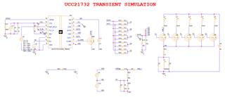
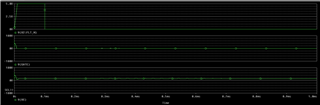
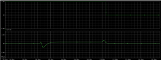
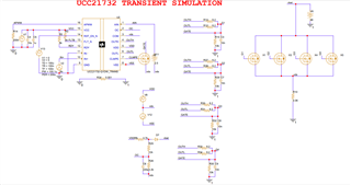
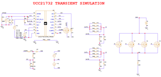
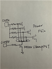
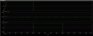
I'm currently working on Isolated gate driver design and I'm using UCC21732-Q1 to control the MOSFETs. While performing simulation in PSPICE, I see gate remains in HIGH state and FLT pin goes low when the IN+ changes the state from LOW to HIGH.

What might be the reason?

Any suggestions UCC21732-Q1DW_TRANSwould be appreciated.

Thanks.

  • Hi Anand, 

    I think the reason might be the power supply for the primary and the secondary side - looks like they are tied together with a 1kV supply; this explains why the gate voltage is -1kV when you're measuring it against the primary side GND. Also it makes it harder to see whether the gate is actually switching when the IN+ turns on. 

    You can try tying the two GNDs together first and see if the simulation runs correctly; I would also suggest probing the OC pin, since overvoltage on the OC pin would cause the nFLT pin to go low. 

    Hope this helps! 

    Thanks, 

    Vivian

  • Thanks for your input Vivian,

    I tried removing the 1kV supply between the GND and simulated. Still I'm seeing the same error. But, when I remove the DESAT circuit then the circuit works as expected.

  • Hi Anand, 

    In that case, I would look into the design of the OC-as-DESAT circuit as well as the parameter for other components in the system. For example, you can look into the Vds voltage of the FET when the gate driver turns on; if the Vds of the FET during initial turn-on exceeds the DESAT detection threshold and the blanking capacitor is small, that might explain why there's DESAT triggering. 

    You can use the UCC217XX calculator linked here in the product page to calculate the detection threshold and blanking time. 

    Alternatively, you can try using the UCC21750 simulation model. UCC21750 has DESAT function with a leading edge blanking time; that means it will ignore Vds overvoltage for the first ~200ns after the gate turns on to prevent false DESAT triggering. 

    Hope these suggestions help! 

    Thanks, 

    Vivian

  • Hi Vivian,

    I think I found the issue, the DESAT circuit was connected to VDD instead of VDS. After doing the change circuit is working as expected.

    I just have few doubts.

    • what's the actual difference between DESAT config and OC using DESAT config?
    • whether can I remove miller clamp MOSFET when I'm using Bi-polar supply?
    • On what basis VOCDET value is chosen?

    Thanks,

  • Hi Anand, 

    To answer your questions - 

    1. Both of these methods depend on the Vds/Vce of the FET/IGBT to detect over-current and short-circuit conditions. The detection timing is a bit different between these two approaches, and the required external components are also different. Usually, OC-as-DESAT would need additional current to charge the blanking capacitor, while DESAT itself has 500uA of DESAT current. You can choose these two approaches based on your preference. 

    2. Miller clamp is suggested either way, whether you're using a negative bias supply or not. The reason being that the board pasitics together with the Miller capacitance might create voltage spikes exceeding the threshold voltage even with the presence of a negative bias supply. For this family of smart isolated gate drivers, we have versions with the internal Miller clamp (for example, UCC21710 and UCC21750) if you don't want to use an external Miller clamp FET. 

    3. The OCDET detection threshold is calculated using the method mentioned here, essentially take into consideration of the voltage drop across various external components (resistors, diodes, etc,) 

    Hope this helps! 

    Thanks, 

    Vivian

  • Thanks for the detailed explanation Vivian,

    As my circuit is working as expected with OC as DESAT functionality. I wanted to perform some stress analysis for my MOSFETs. I remember PSPICE has SMOKE analysis to do stress analysis but whether PSPICE for TI has the same?

    If not, is there any method to perform stress analysis or worst case analysis for the MOSFETs in PSPICE for TI?

  • Also, I'm trying to vary VOCDET by varying desat network parameters but, in simulation, voltage at OC pin is not rising more than 0.7V 

    Is it okay to have VOCDET value close to VOCTH?

  • Hi Anand, 

    I'm not sure of the particular analysis you talked about - perhaps you can post another question in the PSpice for TI forum, and an expert can help you out. 

    VOCDET means the Vds/Vce voltage at which the OC pin triggers. The OC pin always triggers and initiates soft turn-off/two level turn-off at ~0.7V, but with different external components, the Vds/Vce threshold at which the turn-off event happens is different. Thus, you should find a Vds/Vce level at which you consider the FET/IGBT is short-circuited, and adjust the external component value to make sure OC gets triggered at the desired Vds/Vce voltage. 

    Thanks, 

    Vivian

  • Okay, I will try opening a new case for that. 

    Thanks for your support Vivian.

  • You’re welcome - anytime! 
    Vivian

  • Hi Vivian,

    I'm planning to drive 4 MOSFETs in parallel using single gate driver. Individual Gate resistors are used for both Sink and Source of individual MOSFET. But how to connect the CLMPE pin. Whether can i short all the Gate signals and connect to Miller Mosfet ( as shown in the below image)? or any other method to connect these signals?

  • Hi Anand, 

    I would not recommend connecting all the gates together - parameter mismatch of the FETs might cause undesired oscillation of the gate. 

    If you desire to utilize the Miller Clamp function, I would recommend using different Miller Clamp FETs, one for each power MOSFET you're driving. The CLMPE pin can be connected to the gates of the Miller Clamp FETs with a small gate resistance (<10 Ohm or so). 

    Hope this helps! 

    Thanks, 

    Vivian

  • Thanks for your feedback. Will it be an issue if i use single miller MOSFET? I'm little worried about space.

  • Hi Anand, 

    You can experiment with a single Miller clamp FET, though it's not recommended. I would recommend leaving footprint for the extra Miller clamp FETs and not populating them for the prototype board if possible.  

    If you're really tight on board space and don't find the single Miller Clamp FET approach effective, worse case you can use bipolar bias supply and make VEE larger to hopefully mitigate any false turn-on issue. 

    Hope that helps! 

    Thanks, 

    Vivian

  • Hi Vivian,

    I'm considered bi-polar supply of +15V and -8V. So I hope this should be sufficient for the driver to prevent false turn-on?

    And as you said earlier, "I would not recommend connecting all the gates together - parameter mismatch of the FETs might cause undesired oscillation of the gatewhat if I connect all the gates together and place individual gate resistors near to each MOSFET. Still, will there be undesired ringing?

  • Hi Anand, 

    In order for the Miller clamp to be effective, no resistance should be added on the Miller Clamp path. The drain of the Miller clamp FET should be directly connected to the gate of the power MOSFET to provide a low impedance path in the case of false turn-on. Even if you have separate gate resistors, it would not separate the gate on the Miller clamp path. 

    +15V/-8V should be good enough to solve majority of the false turn-on issue in my opinion. 

    Thanks! 

    Vivian

  • Hi Vivian,

    Those resistors (8.2Ohm) are for source/sink functionality not for CLMPE. Anyhow Miller Clamp path won't be having any resistors. So this should be fine right?

  • Hi Anand, 

    This is what I mean - even though you have separate resistor per power FET from OUTH/OUTL, if you're just using one Miller Clamp FET, you're connecting all the gates together to the Miller Clamp FET drain. So if you're just using one Miller Clamp FET, having separate gate resistor doesn't separate the gates. 

    Vivian

  • Okay. But, all 4x MOSFET are considered as single power MOSFET in the design. So all of them will be turning ON/OFF synchronously. In this case, having single clamp MOSFET for all gate 4x shouldn't be an issue right?

    Sorry if I'm confusing this more.

  • Hi Anand, 

    Theoretically, it should not be an issue if all the FETs and gate resistors have the exact same parameters. However in real life they are never completely the same, and the FETs are placed at different places on the PCB so the different parasitic capacitance/inductance of the PCB come into play as well. 

    I would say - try simulating it by varying the FET parameters a little bit (internal gate resistance, gate capacitance, etc.) for each FET. If no major issue occurs, you can try this approach in the actual PCB. Worst case would be there's gate ringing to disrupt normal performance; in that case you can just choose not to use CLMPE, since you have +15V/-8V bipolar supply. 

    Vivian