This thread has been locked.

If you have a related question, please click the "Ask a related question" button in the top right corner. The newly created question will be automatically linked to this question.

LM51571-Q1: Proper use of Webench Power Designer

Part Number: LM51571-Q1
Other Parts Discussed in Thread: LM5157

Hello,

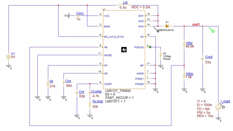
I need following conversion Vin = 5V, Vout = 40V, Iout_max = 150mA. I enetered them in Webench Power Designer.

Webench Power Designer poroposed several solutions.

Good compromise among all solutions (in term of IC temperature and number of components) was LM51571.

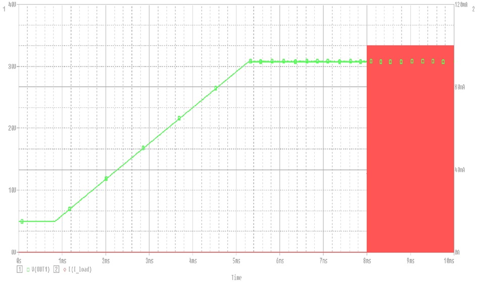
But output ripples were quite significant for my app - more than 100mV.

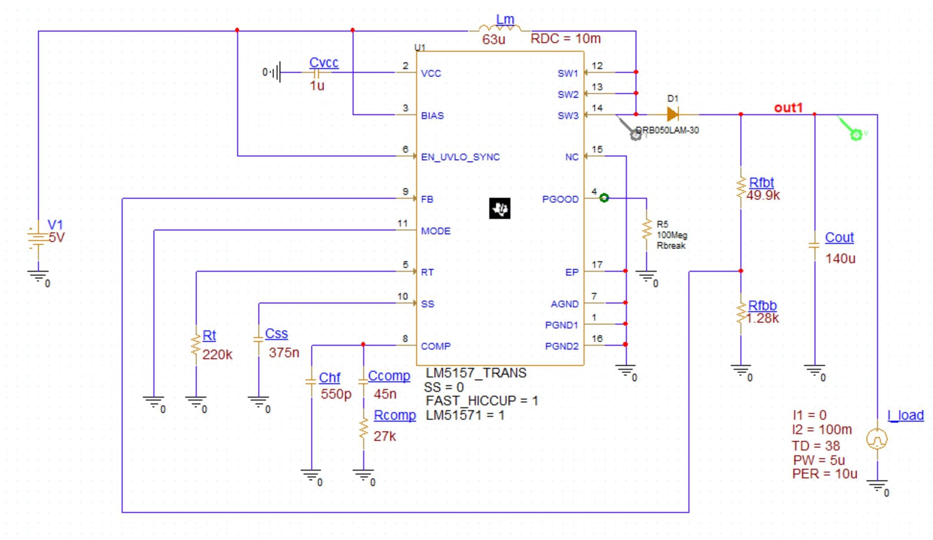
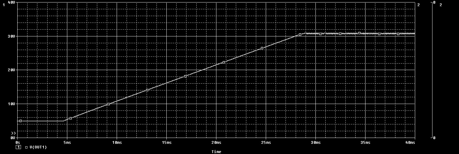
Should I refine component values in simulations (transfering schematic in Pspice for TI) or deos exsit method to limit ripples in Webench Power Designer.

Thanks in advance.

Pavel.

  • Hi Pavel,

    Thanks for using the e2e forum and our webench tool.
    I agree that LM5157 should be a good and efficient part selection for your parameters.

    The output voltage ripple is mostly dependent on the output capacitance, inductor and switching frequency.
    To find the best modification to reduce output ripple, I recommend using our quickstart calculation tool for LM51571:
    https://www.ti.com/tool/download/SNVR511

    This tool takes more inputs than webench, so further finetuning is easier.
    You are also able to set a desired output ripple limit and get according recommendations on output capacitance.

    Please let me know if there are additional questions or design review requests.
    Best regards,
    Niklas

  • Hi Niklas,

    Thanks. Did as you suggested, but simulation check failed.

    Here is schematic with components paranetrized according exel tool:

    6253.schematics.pdf

    Here is simulation:

    transient_200us.pdf

    and here is excel ...

    LM5157-58_v0.xlsx

    Where did I go wrong?

    Thanks.

    Pavel.

  • Hi Pavel,

    There are some optimization I can propose for this design.

    - The boost ratio from 5V to 40V requires a high duty cycle, which is very close to the device limits when operating with maximum duty cycle of 2.1MHz.
    To guarantee the device is able to provide the required duty cycle, I would recommend a lower fsw. E.g. 400kHz.
    - To reduce current ripple, the inductance can be increase. (Especially when fsw is reduced, a higher inductance is required)
    - The suggested output capacitance is only the minimum value required for a stable system. You can increase output capacitance further and and bulk capacitance to reduce output ripple and improve transient performance.

    Best regards,
    Niklas

  • Hi Niklas, 

    I did the modifications you proposed. It didn't help.

    I think that there is something wrong with model as it seems that MOSFET switches in regulator model don't work: the current I measured in simulation is 0 on pins 12, 13, 14 (i.e. SW1, SW2, SW3). What signify parameters 'SS' (which is set to 0) and 'FAST_HICAP' (which is set to 1) for the model LM5157_TRANS that I use in my simulation ?

    Sincerely,

    Pavel

  • What is the difference between LM5157_TRANS and LM5157_AVG ?

  • Hi Pavel,

    Thanks for the update.
    If you do not measure any current going into the switch pin, the device seems to be inactive and not switching.
    Has this always been the case, or was the device switching in previous simulations?

    You can also use the default testbench that comes with the PSpice files for reference.
    This design should work properly.

    The LM5157_TRANS is the transient model, which is meant for steady state and transient simulations.
    The LM5157_AVG is the average model for bode plot and stability analysis.

    Best regards,
    Niklas

  • Hi Niklas,

    At first the simulation seemed a little better.
    The output wasn't 40V (as the tool calculated), but it wasn't 5V either, if I remember correctly just over 10V.
    I didn't measure the current at SW1, SW2, SW3, but I think they worked.

    At the same time, I noticed that the GNDs are not at 0 V, but at a negative value.
    Then I replaced all the GNDs with GNDs featuring “0”.
    After that, all GNDs were at 0V, but the output was at 5V (without load current) and less than 5V with load current.

    Sincerely,

    Pavel.

  • I understood what happened: design parameter "start-up time" (defined by Css) was larger than simulation time.

  • Hi Pavel,

    Please allow us some time to get back to you. 

    BR,

    Haroon

  • Hi Haroon,

    Thanks. The problem I talked previously can be considered as resolved: my simulation time was too short.

    But there are other problems: I can't reach 40V at output. I used different combinations of RFBB and RFBT to get 40V, but it seems that device limits output at about 30.7V.

    For example in my last simulation case with RFBB = 1kΩ and RFBT = 49.9kΩ, the Vout should be 51V (according to the equation 9 om page 23 of datasheet: 1V * (49.9/1 + 1) = 51. But it is at 30.7V.

    I also used different strat-up times playing with Css (finally accepting quite huge strat-up time, suggested by Excel tool), but it didn't help.

    Where is the problem ?


    Here is my simulation case:

    And here are results:

    P.S. By the way, I couldn't display the current on the SW3 pin... there was simply no option to select it using "Add Traces". Is this a tool bug?

  • Hi Pavel,

    Please allow us some time to get back to you, our bandwidth at the moment is quite narrow so we would need some time to get back to you.

    Thanks for understanding.

    BR,

    Haroon

  • Hi Pavel,

    Sorry for the long delay on this case.
    First of all, I am glad to hear you found and correct the initial error of GND reference and  softstart time.

    Regarding the output voltage:
    It seems like you are hitting the maximum on-time limits of the device. The datasheet lists that at higher fsw, the worst case maximum duty cycle is only 80%.
    Boosting from 5V up to 40V would require a duty cycle of ~87%.
    If you zoom in to the switch note voltage of your simulation, you can see the actual duty cycle the device is switching with.

    The fastest way to achieve a higher duty cycle is by reducing the switching frequency.
    You can test the same setup with a 100kHz switching frequency (increase Rt to 220kOhms). You might need to adjust the inductance and compensation as well, but this way you should be able to achieve the desired 40V on the output.

    If the duty cycle is still too high for the device and the output voltage can never be achieved, you might consider changing the topology to a flyback with adjusted winding ratios to reduce the duty cycle.

    Best regards,
    Niklas

  • Hi Niklas,

    I did as you suggested. Nothing changed !!! The output is still stucked at this "magic" value of about 30.7V.

    This may be a bug in the tool.
    I could not display the current at the SW3 input... although I put the current probe on SW3 (pin 14), I did not find it in the list of measured values at the end of simulation.
    In my setup I use an external diode model. The tool indicates that in such cases the number of probes is limited to 3.
    Before I put 3 probes - Vout, Iload and Isw3, but Isw3 I was never able to select at the end of the simulation.
    Last time I removed Iload, leaving only Vout and Isw3, but again I was unable to display Isw3.

    In my last setup I adjusted Rt, Lm to get 100kHz switching frequency and also adjusted loop compensation values (as tool suggested). The tool is also suggested to increase Css until 373nF that increased considerably simulation time until 40ms, but I did it anyway.

    Here is my last setup:

    And here is simulation:

    Sincerely,

    Pavel.

  • Hi Pavel,

    Please allow us some time to get back to you.

    Thank you

    BR,

    Haroon

  • Hi Haroon,

    Ok, thanks.

    Sincerely,

    Pavel.

  • Hi Pavel,

    I tested on the default bench, if a boost ratio from 5V to 40V can be achieved.
    The simulation worked fine and the output goes up to 40V as desired.
    I attach the model here, so you can use this testbench for reference.

    7446.LM5157_PSPICE_TRANS.zip

    Please note that I set a very small softstart cap, so the 40V output is reached within 3ms. This now leads to an overshoot at the output and the device goes into standby temporarily until Vout goes back down.
    If the increase the SS cap again, the device should start up normally without resetting.

    Best regards,
    Niklas

  • Hi Niklas,

    Thanks. I understood what caused problem: model of external diode.

    When I replace it with ideal diode (as in you example), it's Ok.

    Here is this model:

     * DRB050LAM-30 D model
    * Model Generated by ROHM
    * All Rights Reserved
    * Commercial Use or Resale Restricted
    * Date: 2019/04/08
    .MODEL DRB050LAM-30 D
    + IS=957.78E-9
    + N=0.9340
    + RS=4.8265E-3
    + IKF=141.25E-3
    + XTI=2.0
    + EG=0.700
    + CJO=1.2667E-9
    + M=0.5574
    + VJ=0.5000
    + ISR=3.4880E-6
    + NR=1.2143
    + BV=30
    + TRS1=2.7980E-3
    + TIKF=15.384E-3

    Any comments ?

    Thanks once more.

    Pavel.

  • Hi Pavel,

    Please allow us sometime to get back to you on this.

    BR,

    Haroon

  • Hi Pavel,

    Thanks for the update.
    I am glad to hear that you found the error in your model.
    I cannot say what exactly cause the output voltage to drop based on the model specs.
    My first guess would be a wrong current or voltage rating that cannot support the application.
    You can import another diode model and see if the simulation improves.

    Best regards,
    Niklas