This thread has been locked.

If you have a related question, please click the "Ask a related question" button in the top right corner. The newly created question will be automatically linked to this question.

LM5155: LM5155 does not start in flyback and boost configurations

Part Number: LM5155

Hi,

I need a +/-135VDC power supply (at around 30-35mA for each output) for one of the our projects.

I thought of using LM5155 in flyback and boost topologies.

I've built an eval. board (see attached pdf) for both configurations to proof the concept before using them in project, but non of them even start.

I tried different values for RT and SS pins, connected UVLO directly to BIAS and for flyback configuration added and optional PNP transistor on primary side as shown in data sheet.

I saw recommendations on using zener on the secondary side for flyback configuration, but didn't try it yet since the boost topology, where there is no secondary side, does not start as well.

Also, tried bypassing EMI filter.

No luck, I just can not get them started for both configurations.

Can you please check the schematics, what can be wrong there ?

Thanks !

SCH_LM5155_Eval_Board.pdf

  • Hi Ashot,

    Thank you for using E2E forums, regarding your query please could you fill out this excel sheet calculator tool with your design specs? https://www.ti.com/tool/download/SNVC240 

    BR,

    Haroon


  • Hi Haroon,

    Thank you for the prompt reply.

    Please find attached the excel files for both configurations. I tried to fill them out to the best of my understanding.

    Thanks again,

    Ashot

    Copy_LM5155_56_Excel_Quickstart_Calculator_for_Flyback_Regulator_Design (version 1).xlsx

    4130.Copy of LM5155_56_Quickstart_Calculator_for_Boost_Converter_Design_V1_1_1.xlsx

  • Hello Ashot,

    Let's concentrate on the boost converter first.

    It seems that you are having very low input capacitance compared to your output capacitance. Please try to add a big capacitor there.

    How does the startup of the converter look like, when you apply the 24V? Please share some scope plots at startup. Please use all 4 channels of the scope and share at least one channel if you are sending several scope pictures. Have a look at the signals you mention above as well as the gate drive and the COMP voltage. Input and output voltage would be good as well.

    Best regards,
    Brigitte

  • Hi Brigitte,

    Thank you for the help.

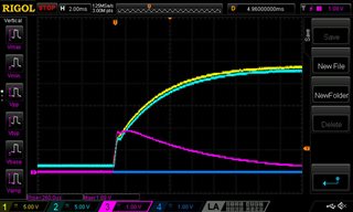
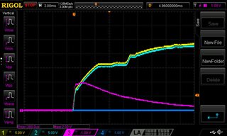
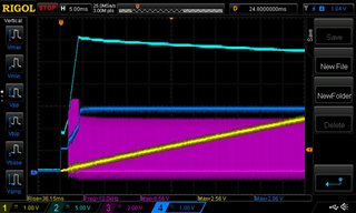
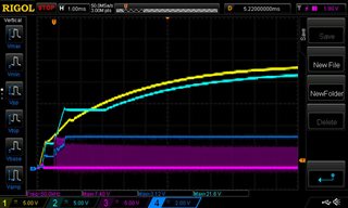
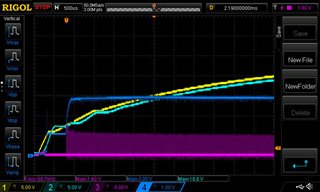
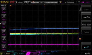
    I added 2x47uF capacitors on input , before EMI filter (pic NewFile1a) then moved them to after EMI filter (pic NewFile1b).

    In both cases COMP voltage is around GND and Gate Voltage never reaches the ON threshold for the MOSFET, which is around 4V.

    Yellow - Input Voltage;

    Cyan - Output Voltage;

    Magenta - Gate Voltage;

    Blue - COMP Voltage;

    Thanks again,

    Ashot

  • Hello Ashot,

    COMP to GND means the converter is operating at 0% duty cycle. Can you please check the SS voltage during startup?

    Is it possible that you have a connection issue with the FB pin?

    Best regards,
    Brigitte

  • Hi Brigitte,

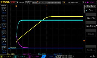
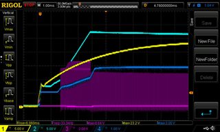
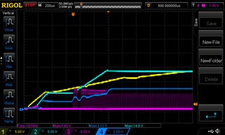
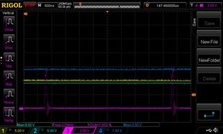
    I captured SS voltage at startup, it goes up to around 5V (see yellow line, pic NewFile1c).

    FB pin connection looks ok and I measure there around 1.18V.

    Yellow - SS pin;

    Magenta - Gate;

    Blue - COMP;

    Cyan - Output;

    Thanks and Regards,

    Ashot

  • Hello Ashot,

    If you measure 1.18V on the FB, the output is higher than the set level and the device will not switch. The FB voltage is at 1V during normal operation.

    Best regards,
    Brigitte

  • Hi Brigitte,

    I replaced the Rfbb by 820 Ohms (it was 1.2K), but it didn't help.

    Same behavior, except I measure 0.7972V now at FB pin.

    Anyway, what are feedback resistor values for 135V output ?

    According to data sheet formula, it should be e.g. Rfbt=135K and Rfbb=1K. 

    Thanks,

    Ashot

  • Hello Ashot,

    For the feedback divider values, please have a look at this app note: Design considerations for a resistive feedback divider in a DC/DC converter

    Is it possible that due to anything strange happening, the LM5155 is damaged in your test board? What happens if you exchange the IC?

    Please measure as well the input voltage when you start up the converter and send the measurement result.

    Best regards,
    Brigitte

  • Hi Brigitte,

    I ordered some spare parts and will let you the results as soon as they delivered/replaced.

    Thanks for the help and Regards,

    Ashot

  • Hi Brigitte,

    Looks like you were right, the IC was probably damaged somehow. After replacing it the switching starts but still no proper regulation on the output.

    With the current feedback resistors combo I should have around 109V but I still have something around 23.2V (looks like input 24V minus voltage drop over rectifying diode).

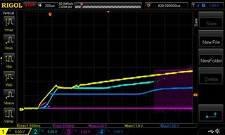
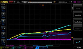
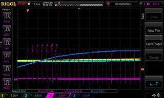
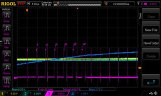
    Here are some scope screen pics of switching and on start up:

    Cyan - output;

    Yellow- SS pin;

    Blue -COMP pin;

    Magenta - Gate;

    Changed Yellow beam to Input:

    Switching frequency is 220KHz, but pulse width is only around 150nS. I suspect it is the issue, no enough time to boost the output voltage.

    What would you advise ?

    Thank you and Regards,

    Ashot

  • Hi Ashot,

    Thanks for your response and for the scope screenshots. We will get back to you with a reply by tomorrow.

    Thank you and best regards,
    Bryan

  • Hi Ashot,

    Sorry for the long delay on this.

    It is good to hear that the device is turning on now and starts to switch.
    It seems like it starts to boost correctly at the beginning and the just stops.

    I checked once more the calculator sheet values you attached.
    It seems like the file is corrupted and the bode plot is not calculated correctly.
    I re-entered your specs and it showed that the design has rather low stability:

    We recommend at least 60 degree phase margin for a stable system.

    I would recommend to adjust the compensation and check if the regulation improves.
    If possible, you can also add the recommend high frequency cap C_hf in parallel to the RC.
    The calculator also recommend a slope compensation resistor, as subharmonic oscillation can be a risk for duty cycles >50%.
    Your current schematic does not show a placeholder resistor directly at the CS pin, so I am not sure if it is possible to add such a resistor to your design.

    Also, please make sure to check the bias derating and ESR of your output caps.
    The actual capacitance might be lower at 135V bias.

    If there is no improvement, we might need to look once more into the switch node signal to check if we see an irregular duty cycle or oscillation,
    and also check if the FB and COMP signals are abnormal.

    Thanks and best regards,
    Niklas

  • Hi Niklas,

    Thanks for the response.

    I tried the newer suggested values for the COMP pin (100K plus 10nF), but it didn't help.

    I also replaced the 0.47uF on SS pin to 0.1uF. I did not add Chf and Rsl yet.

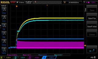
    No much difference in behavior, here are the screen shots:

    Yellow- Input;

    Cyan- Output;

    Blue- COMP;

    Magenta- Gate;

    You can see a gap in Gate switching waveform at the startup.

    After adding two more 4.7uF caps on the output the gap is gone but it still does not regulate.

    Here are the pics:

    Thanks and Regards,

    Ashot 

  • Hi Ashot,

    Thanks for trying out the suggestions and adding the new scope screenshots.
    We'll get back to later today with more information.

    Thank you and best regards,
    Bryan

  • Hi Ashot,

    Thanks for the update and the waveforms.
    Let me summarize once more to make sure we did not miss anything:

    - Application is Vin 24V, Vout 135V, Load 50mA
    - This should be a duty cycle ~85%, so we are not hitting the max duty cycle limits of LM5155
    - Compensation network should be stable
    - Comp pin is high and FB pin is below Vref
    - VCC and SS are high, so the device is active
    - The startup is without load, so there should be no risk of overcurrent protection

    Please correct me if any of these statements are wrong.

    The device only boosts up to 13V and then does not achieve boosting anymore.
    It might be the case the inductor cannot deliver the power to the output...
    If the losses in the inductor and schottky diode are too high, the output voltage cannot go up.
    I also noticed the inductor is not shielded. I would highly recommend using a shielded inductor to reduce the noise levels on the board.

    If you zoom in on the gate signal when the device is switching, we can see the duty cycle of the device based on this.
    If it is >85%, we can assume that the required duty cycle cannot be achieved.
    If it is very small, the device might run with overcurrent limitation due to high losses. This would become visible when measuring the CS pin voltage.

    Best regards,
    Niklas

  • Hi Niklas,

    All of your statements above are correct.

    Here are some numbers I measure:

    COMP pin - 2.83V;

    SS pin - 3.49V;

    FB pin - 0.145V;

    CS pin - 0.157V (for both - 120mOhms and 47mOhms values, see below for description);

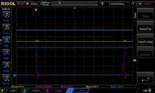
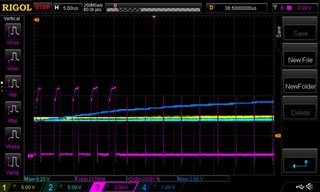
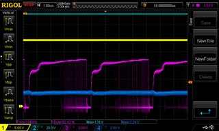
    And here are some scope pics regarding duty cycle at start up and thereafter:


    As you can see duty cycle gets max at around 30% at start up and then comes down to around 1.5%.

    I tried to increase inductance by adding few more inductors in series reaching to around 1.5mH, and also replacing the inductor with the lower value one - 150uH but rated for much higher saturation current. No changes in behavior.

    Most interesting was when I replaced 120mOhms current sense resistor by 47mOhms resistor. For a moment output voltage boosted to quite high level but I was not able to measure or capture it since it lasted only few seconds. I suspected that transistor damaged and replaced it but the output voltage boost never happened again.

    Thanks and Regards,

    Ashot

  • Hi Ashot,

    Thanks for the update.
    The low duty cycle indicates that the device runs in overcurrent protection (OCP).
    The device pulls down the gate signal after the minimum on-time as the voltage at the CS pin is above the OCP trigger votlage (100mV)

    CS pin - 0.157V (for both - 120mOhms and 47mOhms values, see below for description);

    In OCP state, the device does not shut down, but runs with minimal duty cycle instead, which can be seen within the waveforms.

    A higher output capacitance will make this behavior worse, as the device has to deliver more power to the output to charge the caps, which results in even higher currents.

    To solve this issue, it would be required to:
    - increase softstart time with larger SS cap.
    - Reduce CS resistor. (you already reduced to 47mOhm, which is better than 120mOhm)

    The votlage at CS pin should not go above the 100mV limit, neither during ramp-up phase, nor during steady-state operation.

    Best regards,
    Niklas

  • Hi Niklas,

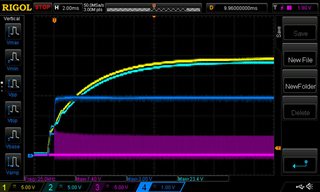
    Glad to let you know that it finally worked.

    I removed one of the 4.7uF output caps and increased the SS cap to 1uF.

    Here is the scope pic:

    This was for +135VDC@50mA part of the power supply.

    Now, can we please check the flyback part? Can you please check for recommendations/comments assembling ?

    I want to have clean assembly on another board.

    Thanks a lot and Regards,

    Ashot

  • Hi Ashot,

    Thanks for the feedback, glad to see that it's working.
    Please allow us some more time to look at the flyback part of the design.

    Thank you and best regards,
    Bryan

  • Hi Ashot,

    Regarding the flyback design, I went back to the original schematic and calculator you attached.

    The transformer of 40uH and 1:10 (primary:secondary) winding ratio should be a suitable choice. Sense resistance of 47mOhm look okay as well.
    A problem I noticed here is that no softstart is implemented.
    More information can be found here:
    https://www.ti.com/lit/an/snvaa44/snvaa44.pdf


    Also the resistor R9 might be too large for the LED resistance. A resistance of ~5kOhm might improve the regulation.

    Best regards,
    Niklas