- Ask a related questionWhat is a related question?A related question is a question created from another question. When the related question is created, it will be automatically linked to the original question.
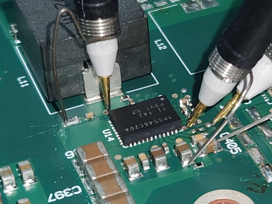
I am facing two issues with TPS546C20A on a single phase design.
Input: 12V
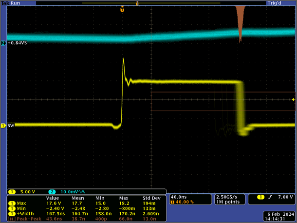
Output: 0.845V 30A
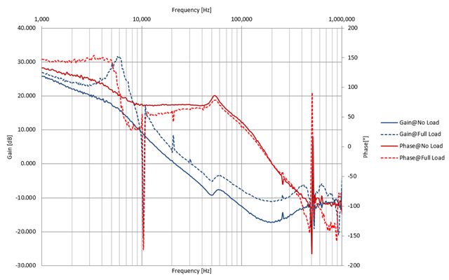
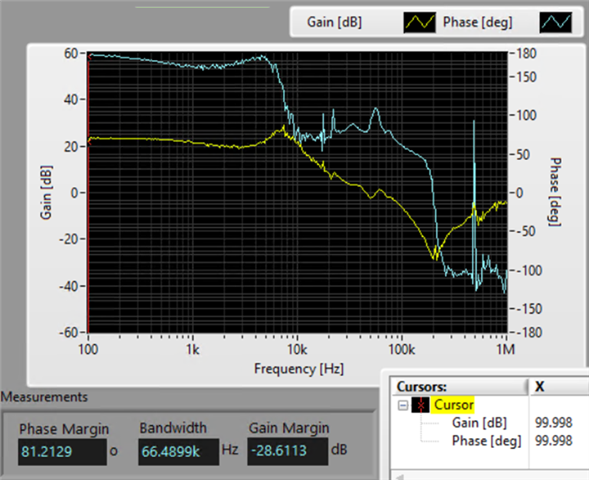
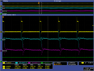
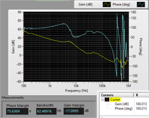
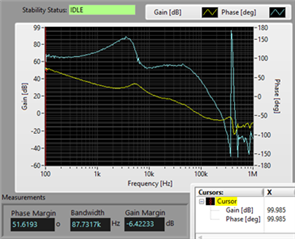
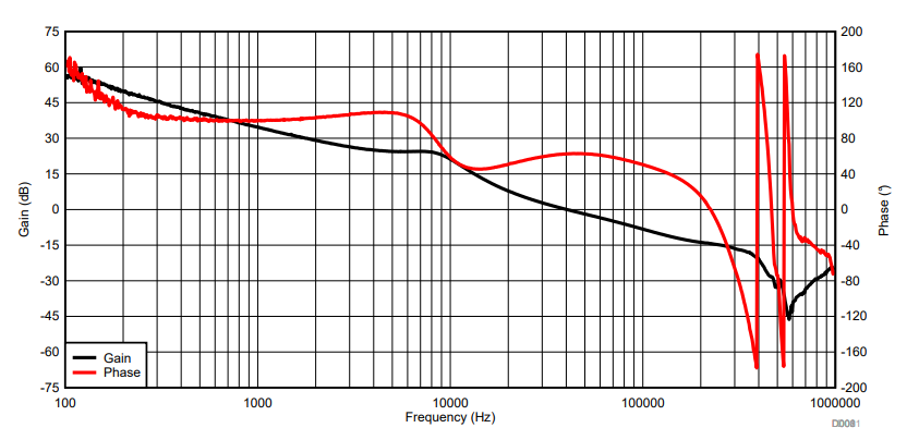
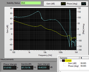
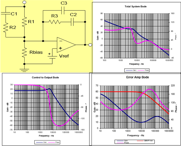
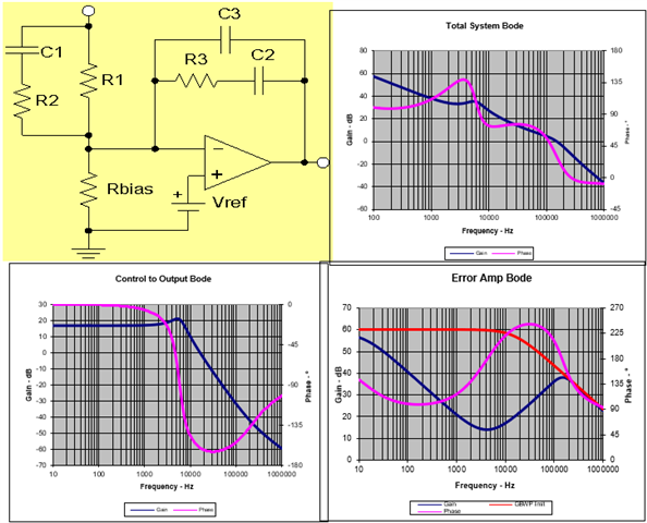
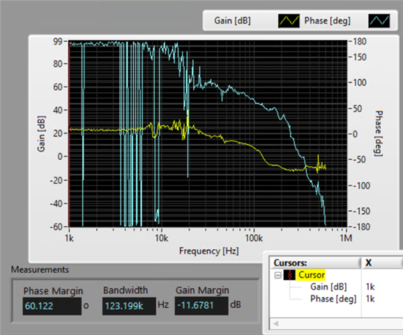
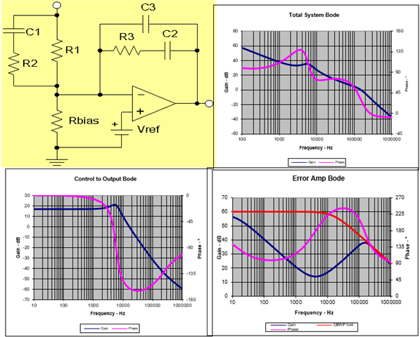
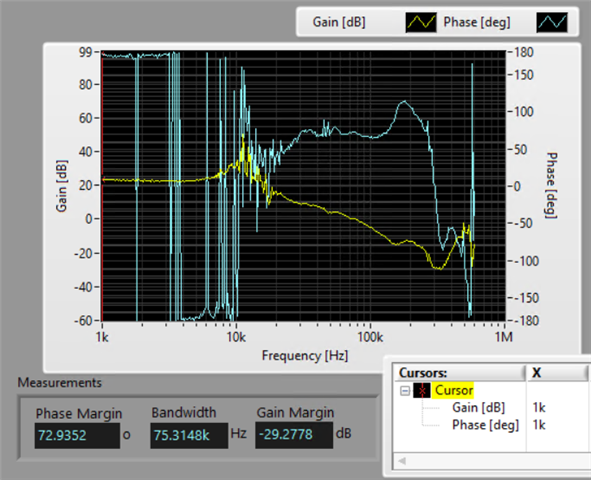
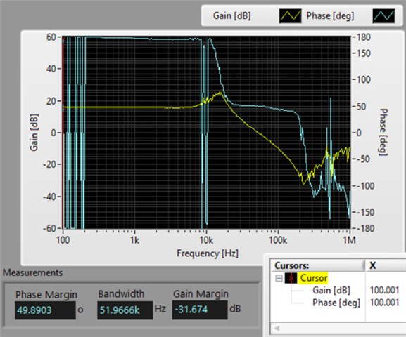
Issue 1: On the measured loop gain, at the low frequency region (1kHz to 4kHz, see Case 4 below for 100Hz to 4kHz), there is no -20dB/decade slope, unlike the designed loop gain bode plot. Type-3 Op-Amp compensator should have a pole at origin that sets a high low-frequency gain and initial -20dB/decade roll-off. What could contribute to a zero at low-frequency to cancel this origin-pole?
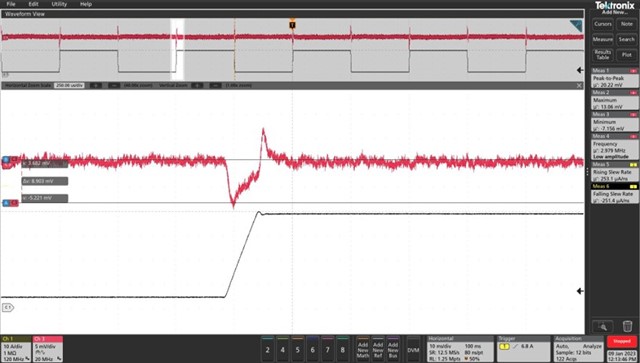
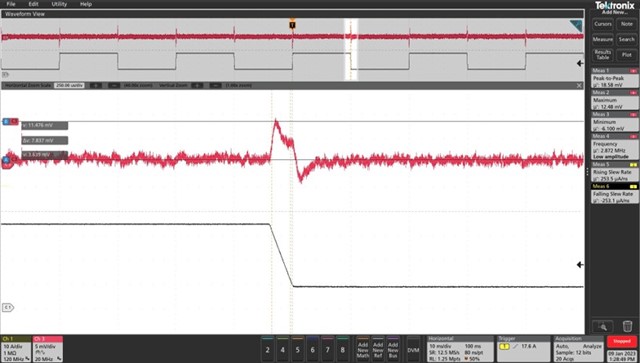
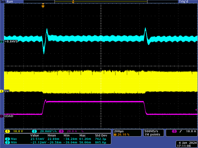
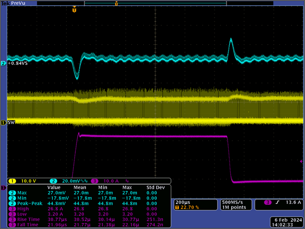
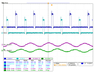
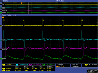
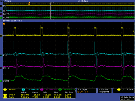
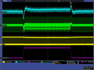
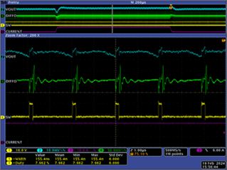
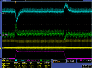
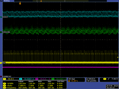
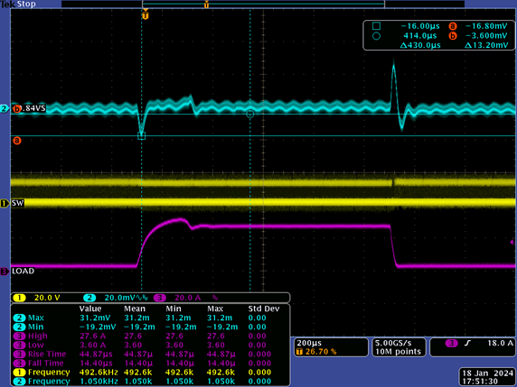
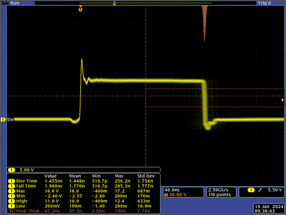
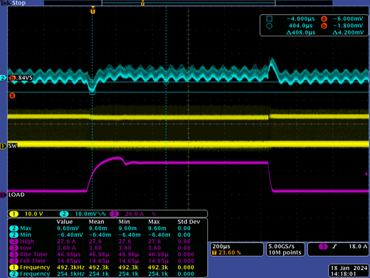
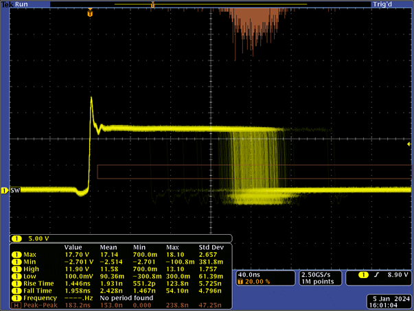
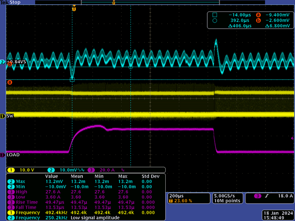
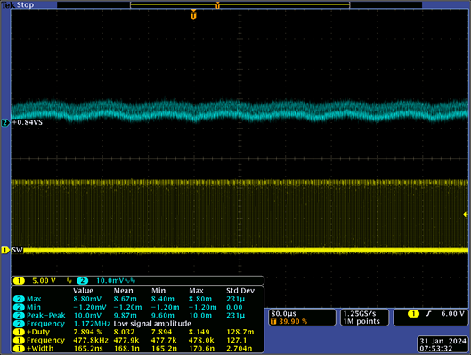
Issue 2: On top of the switch node synchronized output voltage ripple, there is a low-frequency wave, this indicates the control loop is oscillating although with small amplitude. Where does this oscillation comes from, even when the power supply loop gain is designed and tested to be stable with sufficient phase and gain margins?
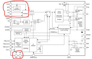
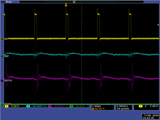
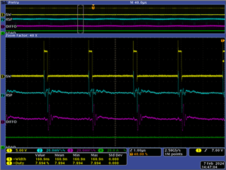
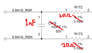
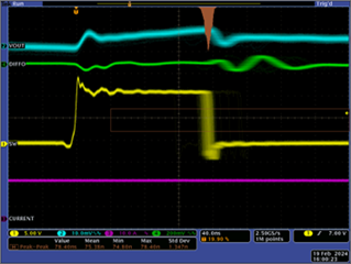
50Ω is placed series on RSN and RSP lines, with 100pF between them as a remote sense filter. The circuit has been tested with different set of instruments i.e. power supply, electronic load, oscilloscope, probes, and still exhibits the same oscillating behaviour, thereby eliminating the factor of instruments loading or back-driving the control loop. An attempt to bypass the remote-sense amplifier is done, but the low-frequency oscillation is still present (see Case 4 below).
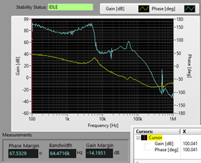
By adjusting the compensation network, below are design and measured data for three cases of loop gain bandwidth on the same power supply.
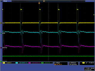
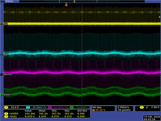
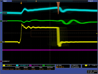
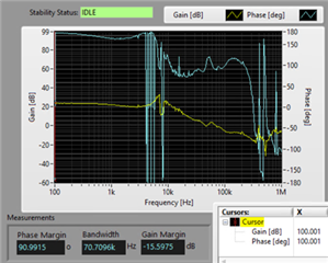
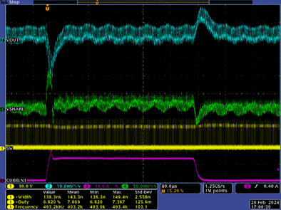
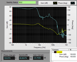
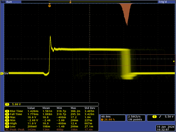
Case 1: Low Bandwidth, Low Jitter, With Low-frequency Oscillation
Attached <SLURB05 — TPS546C20A and TPS546C23 Excel Calculator and Layout Checklist>
TPS546C20A_TPS546C23_Calculator_Checklist.xlsx
|
R1 |
3.74kΩ |
C1 |
1.8nF |
|
R2 |
619Ω |
C2 |
3.9nF |
|
R3 |
10kΩ |
C3 |
100pF |
 |
 |
 |
 |
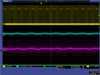
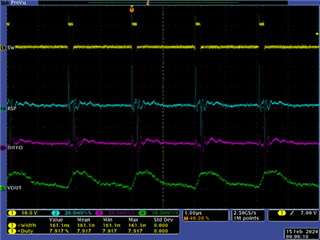
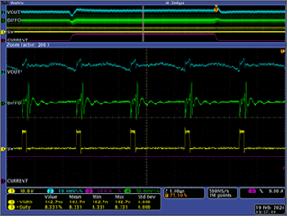
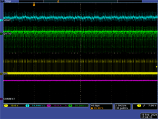
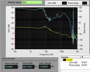
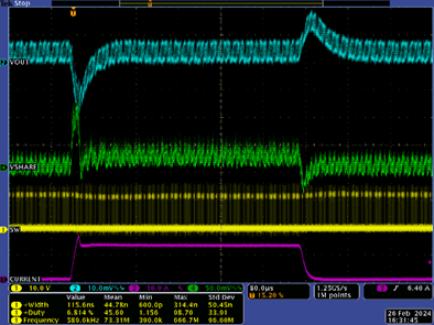
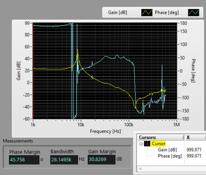
Case 2: High Bandwidth, High Jitter, Also With Low-frequency Oscillation
|
R1 |
3.74kΩ |
C1 |
10nF |
|
R2 |
10Ω |
C2 |
3.9nF |
|
R3 |
10kΩ |
C3 |
100pF |
 |
 |
 |
 |
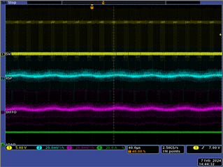
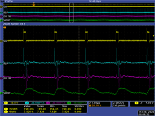
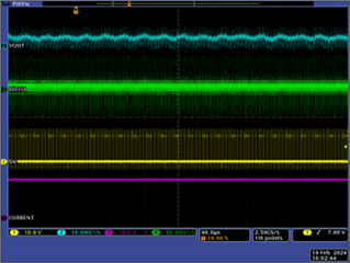
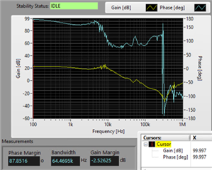
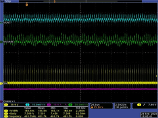
Case 3: Medium Bandwidth, Medium Jitter, Also With Low-frequency Oscillation
|
R1 |
3.74kΩ |
C1 |
3.9nF |
|
R2 |
10Ω |
C2 |
3.9nF |
|
R3 |
10kΩ |
C3 |
100pF |
 |
 |
 |
 |
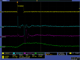
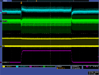
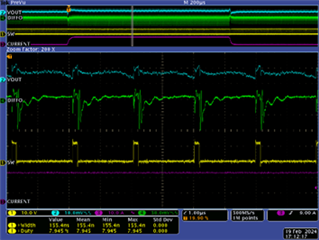
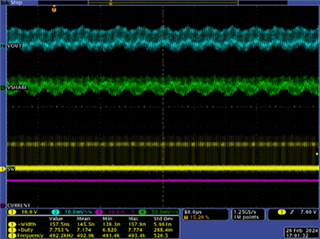
Case 4: Bypass Remote Sense Amplifier (disconnecting DIFFO, RSN, RSP pins and shorting output directly to compensation network)
Still With Low-frequency Oscillation
Compensation network follows Case 1
|
R1 |
3.74kΩ |
C1 |
1.8nF |
|
R2 |
619Ω |
C2 |
3.9nF |
|
R3 |
10kΩ |
C3 |
100pF |
 |
 |