This thread has been locked.

If you have a related question, please click the "Ask a related question" button in the top right corner. The newly created question will be automatically linked to this question.

TPS62932: efficiency

Part Number: TPS62932

Hi

I designed board with TPS62932 and measured efficiency does not meet datasheet's efficiency.
Schematic of tested board:

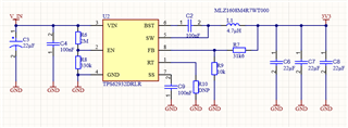
Power supply connected to V_IN
Programmable DC load connected to 3V3
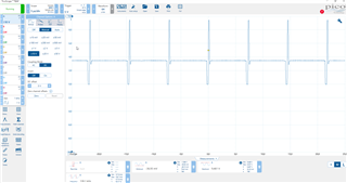
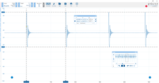
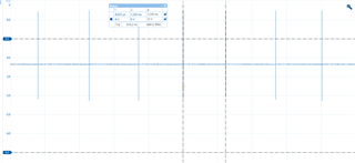
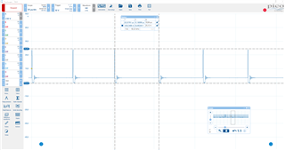
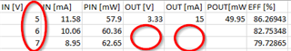
The results:


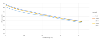
Datasheet efficiency:

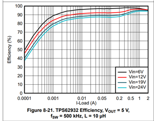
So I expected to have efficiency at least 80% with load current above 10mA.

Do you have any idea why the efficiency is so low?

Best regards
Tomasz

  • Hi Tomasz,

    Thanks for evaluating TPS62932! I think the efficiency gap may come from:

    1. Seems you used a high ESR inductor (MLZ1608M4R7WT000, 500mohm). While our efficiency test used a low ESR inductor (74439346047, 13mohm). So your test condition will have larger inductor power loss, causing lower efficiency.

    You can select a low ESR inductor then re-test.

    2. Please check your measurement accuracy, calibrate the multi-meter equipment first.

    3. You can remove EN-resistors to avoid resistor power loss, our device will be enabled with EN-pin floating.

  • Hi

    Thanks for quick response.

    1) I am aware of ESR of this inductor but with 20mA load the power dissipation on inductor is around 0,2mW which is less than 0,5% efficiency.
    2) Already done.
    3) With 2M and 330k resistors, the power loss for example with 20V input is around 0,2mW which is less than 0,5% efficiency.

    I will try with other inductor and without EN-resistor but I think it is not a problem.

    Best regards

  • Cygan,

    please also review if the VIN is used for U2 (62933) only, in case other components sink more power from VIN cause more input power consumption.

    And also make sure no 3v3 output has no other load on the board except the DC load current you added.

    Yuchang

  • Without enabling Programmable DC load, input current is around 50uA so there is nothing else what can draw current.

  • If you make sure the test data are correct, especially for input and output current. you may check SW mode waveform to review if the IC switching is normal for each load.

  • Hi Tomasz,

    Per Yuchang suggested, please capture SW waveform for us to review, we will check whether device operation is normal.

    Besides, please share your layout file and your efficiency test raw data to us, we will review to find any clues.

  • SW waveform:
    Input 9V, Load:10mA

    Frequency:~138kHz


    Input 9V, Load: 6,66mA

    Frequency:~62kHz


    Input: 9V Load: no load

    Frequency: ~800Hz


    Input:25V, Load: 50mA

    Frequency:~ 92kHz

    Input: 25V, Load: 100mA

    Frequnecy: ~191kHz

    I also tried to catch waveform when the device is switching in designed frequency (500kHz) so I decreased voltage and increased the load.
    Input: 12V, Load: 100mA

    Frequency:~520kHz, Efficiency:66%


    Input: 6,6V, Load: 100mA

    Frequency: ~505kHz, Efficiency:79%

    So with light load the switching frequency is lower than 500kHz as it should, because of PFM mode.

    Efficiency test raw data

    TPS62932_Efficiency.xlsx

    I can share layout files in private message.

    Best regards

  • Hi Tomasz,

    Due to the Chinese New Year holiday until 17/2, we will reply to you later.

    Best regards,

    Zhou

  • Hi Thomas,

    Thanks for sharing the data and layout file.

    1. Seems 5Vin efficiency was close to datasheet value, but with Vin increase, the efficiency gap became larger, right?

    2. Previously you mentioned 50uA no-loading input current, may I know which Vin you tested? Under 5Vin? Could you please measure 5Vin~30Vin no-loading input current?

    3. Seems you only measured Vout once, and didn't measure Vin & Iout. Is the EC-load Iout accurate? Could you use multimeter to measure each Vin/Vout/Iin/Iout value? 

    4. Your first waveform looks wield (I don't understand why low-side FET turned on first, should be high-side FET turn on first). The other SW waveforms look stable.

    5. About your layout, recommend to place the Vout sensing trace after Cout, not before Cout at inductor pad, to get a filtered Vout signal.

    6. Have you tried to change a smaller-DCR inductor?

  • 1. Yes
    2. 45uA-60uA is the current under 5V-25V
    3. I measured vout value with multimeter many times during test and the voltage was changing only a few mV. Also I have checked all other reading with precise multimeter and these values are right.
    6. Smaller DCR inductor I had are too big to fit 0603 footprint. I've tried with different inductor with similar DCR and results are the same.

    I know that smaller DCR inducter would help a little but I dont think that it would increase efficiency by 20%, the output current is very small.

  • Hello Tomasz,

    You can solder the big inductor vertically, only solder one inductor pad, use a wire to connect the other inductor pad.

  • Hello Tomasz,

    Also please check input E-cap (C3) power consumption. High ESR E-cap may cause additional power loss. Please change to MLCC type cap and check again.

  • Hi Tomasz

    I will close this thread now. Please let me know if there are other questions.

    Thanks and best regards.