This thread has been locked.
If you have a related question, please click the "Ask a related question" button in the top right corner. The newly created question will be automatically linked to this question.
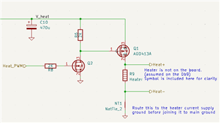
I have a system which controls the temperature of a few Ohm load by intermittently running current though it via a PWM signal to the gate of a MOSFET. I have a large capacitor nearby so that the voltage remains stable. I am considering using the TPS22810 to reduce the inrush current which will be drawn when the circuit is initially connected to the supply.
However I am confused by section 10.4 in the datasheet which recommends an input capacitor 10x as large as the output capacitor. If i need to use a large input capacitor it would invalidate the reason I am using the TPS22810.
Hi Adam,
Such a large capacitor is recommended precisely to reduce the effects of a high inrush current on the input. For your application, a large input capacitor is not required.
Thanks,
Patrick
Thanks for your reply Patrick but what about the concerns in the datasheet regarding flow through the body diode?
10.4
Due to the integrated body diode in the NMOS switch, a CIN greater than CL is highly recommended. A CL greater than CIN can cause VOUT to exceed VIN when the system supply is removed. This can result in current flow through the body diode from VOUT to VIN. A CIN to CL ratio of 10 to 1 is recommended for minimizing VIN dip caused by inrush currents during startup; however, a 10 to 1 ratio for capacitance is not required for proper functionality of the device. A ratio smaller than 10 to 1 (such as 1 to 1) can cause slightly more VIN dip upon turnon due to inrush currents.
Hi Adam,
Will the input supply be removed at all? If the input will be pulled to GND, then some current can flow back through the body diode (depending on the heater resistance). But if the input supply won't be removed while VOUT is high, then this isn't a concern.
Thanks,
Patrick
It is possible, yes. It will be in a card rack and could get pulled. Most likely if this happened EN will also go to 0 at the same time. I was planning on using a suitably small QOD resistor but wasn't sure if the discharge would happen or happen quickly enough in this case.
I'll add that since the output capacitance is large, the QOD isn't so quick. I can't just use the internal one (200 uF Cout limit) so output discharge will be 10s of ms.
Hi Adam,
The other thing to consider here is that if the board gets pulled, will VIN be floating? Or will it have a strong pull-down?
If it will be floating, then a slow discharge won't be an issue because there will be no significant or sustained current from VOUT to VIN. But, if VIN will have a strong connection to GND (>1A instantaneously), then perhaps an input capacitor or PMOS as an extra QOD will be needed.
What do you think about this?
Thanks,
Patrick
I'm not an expert so feel free to correct me.
Hmm... I think that the output capacitor is by far the largest energy source on the board. So I think the input side will discharge more quickly. I am happy to add pull downs, but how large would they need to be? They would need to be quite small to matter discharge the capacitor quickly. If ~250 Ohm I'd be using >0.5W continuous.
What about adding a (beefy) external diode connection Vout back to Vin? This way I'm not relying on / risking the body diode.
It isn't clear to me how a PMOS could be used as a QOD. If I connect VIN to the gate and VOUT to the source I think this would not work; because 22810's body diode probably has a smaller FVD than any PMOS's Vgs.
Hi Adam,
With a PMOS, if you connect the source to VOUT, drain to GND, and gate to EN, then it should be active when the card is removed/EN is at GND while staying Hi-Z when EN is high.
To specify on my statement before, if VIN is floating without a pull-down when the card is removed, then there's no need for worry here because there is no where for a substantial backflow current to, so there would be no substantial backflow current. But yes, a low-FVD diode from VOUT to VIN could be a good safety mechanism to carry any substantial current that might backflow.
Also, it occurred to me that the QOD function might not be desirable in your situation because it would be dissipating power for the low side of every PWM cycle. What you are trying to do here sounds similar to a buck converter - would using one be an option for you? I believe that it would result in higher efficiency and no backflow concerns with similar/lower MCU load.
What are your thoughts about the above?
Thanks,
Patrick
Hi Patrick,
Just to be clear I am not using the device to pulse the heat. A separate MOSFET circuit is doing that. I am only using this chip to slow-charge the large (~2x 470uF) caps.
Its hard to know exactly how fast the input will be pulled down. The 12V input is a power line so it isn't floating, but the rate it is pulled down is hard for me to be sure of. It will depend on the other devices on the board (which will vary from use case to use case for me)
I agree QOD is not useful here but mainly because is not well documented enough to design around for high output capcitance/Vin loss scenarios like I am contemplating.
I may implement a discharge circuit with a PMOS along your lines but the external diode is still required for protection of the device in even of a power low. (worth noting that this will only discharge them down to Vgs)
Thanks for your help! I got it from here.