Other Parts Discussed in Thread: TPS6594EVM
Hi,
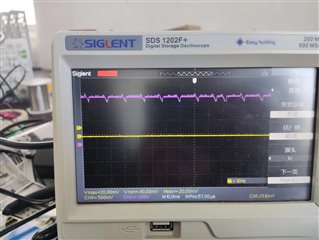
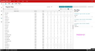
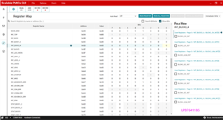
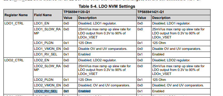
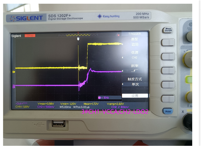
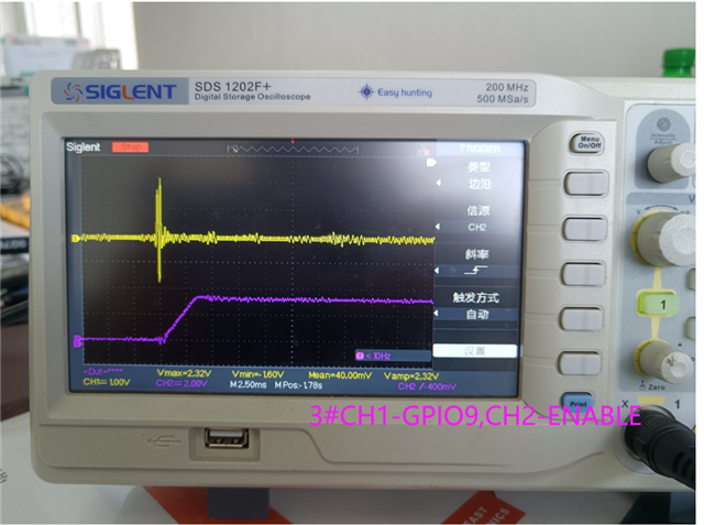
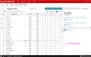
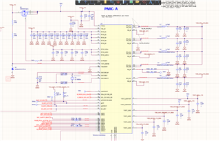
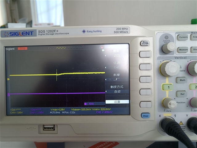
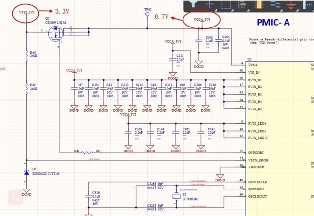
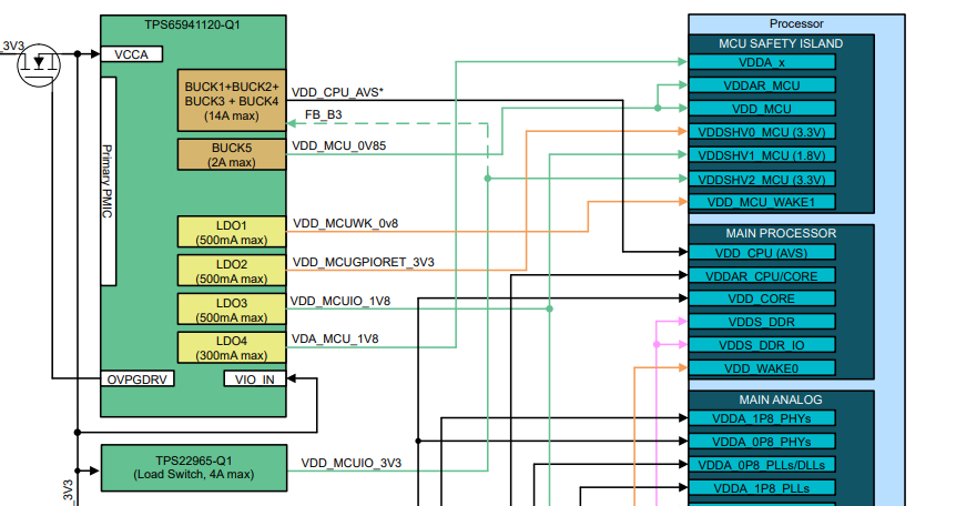
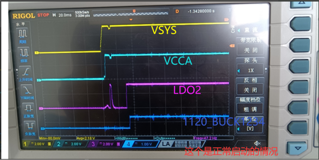
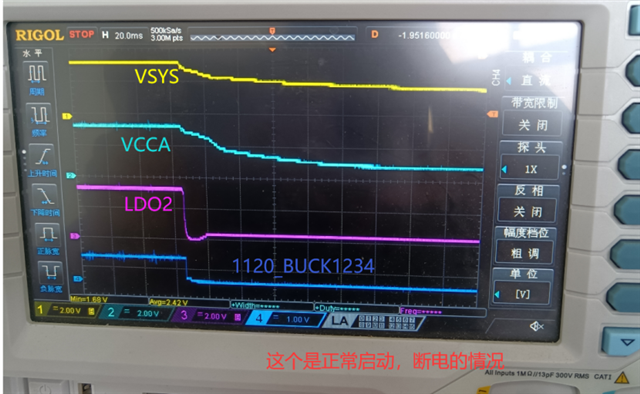
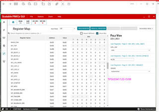
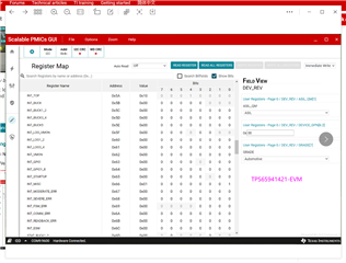
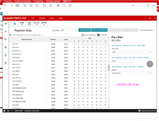
Now we develop our own board by TPS65941120-Q1、 TPS65941421-Q1 and LP876411B5-Q1 PMIC.Now we can read the register content for TPS65941421-Q1 and LP876411B5-Q1 by TPS6594EVM,but can not recognize the TPS65941120-Q1 and so can not read the register content.What is the reason for that? Now I consider some reasons for that.
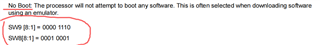
1. The TPS65941120-Q1 peripheral circuit is problematical and the PMIC can not wok.
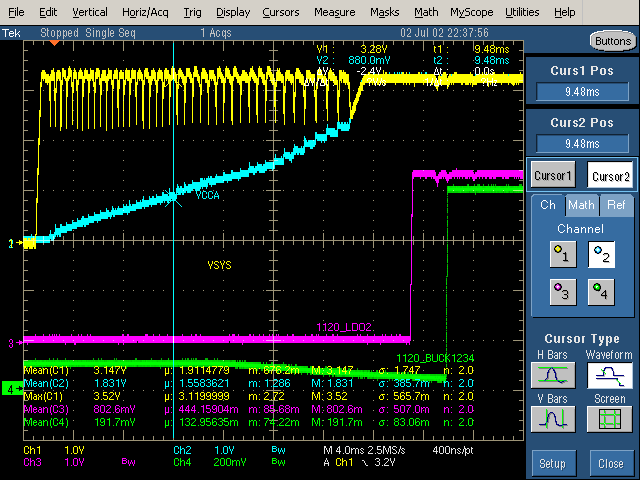
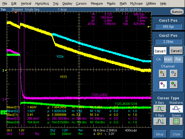
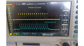
2. The PMIC can work, but not normally and it enters into certain state that I2C can not work well,so we can not recognize the PMIC,but I do not know which state it is.
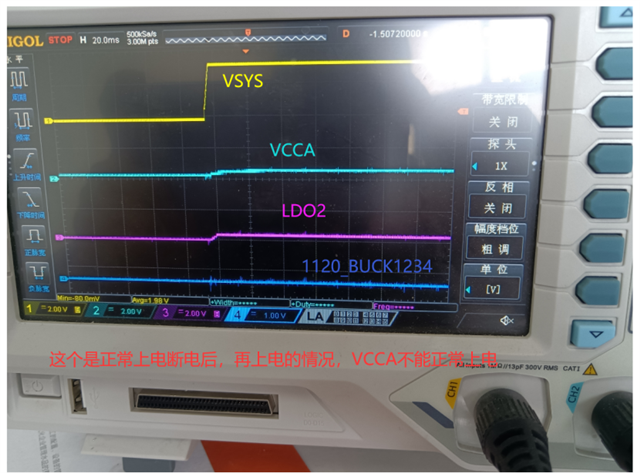
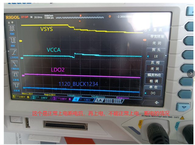
3.The state of the TPS65941421-Q1 and LP876411B5-Q1 PMIC can affect the PS65941120-Q1 PMIC function and make it into certain state that I2C can not work.
BR
Rata