This thread has been locked.
If you have a related question, please click the "Ask a related question" button in the top right corner. The newly created question will be automatically linked to this question.
The layout example in the datasheet can't possibly be correct....
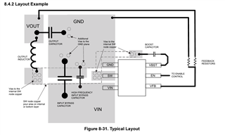
There is vias on the switch node which is going to be a huge issue for emissions.
Is there a reason it was laid out this way?
Nick
Hi Nick,
We have this app note you can refer here, 3 different layouts for SOT family were compared regarding switching spike voltage, thermal, and efficiency.
Optimize DC-DC Layout for SOT Package to Improve Thermal and Voltage Spike
BRs,
Young
Hey Young,
Thank you! Is there a plan to revise the older datasheets with the better version 3 layout? I'm concerned at how many people may be using the original layout.
Nick
Hi Nick,
Thanks a lot for suggestion, we will consider better layout example for future projects.
YZ