This thread has been locked.

If you have a related question, please click the "Ask a related question" button in the top right corner. The newly created question will be automatically linked to this question.

TPS6521905: TPS6521905 Circuit Review Request

Part Number: TPS6521905
Other Parts Discussed in Thread: TPS65220,

Hi, TI expert.

The application the customer is reviewing is cold chain (smart tracker).

At first, we were going to review TPS65220, but TPS6521905 was recommended through E2E, so we will change it to TPS6521905 and review it.

The link to the inquiry previously made to E2E is as follows.

(https://e2e.ti.com/support/power-management-group/power-management/f/power-management-forum/1329416/tps65220-request-a-tps65220-circuit-review-and-related-inquiries-request-a-review)

Accordingly, we would like to request a review of the TPS6521905 circuit.

We request a final circuit review to implement the three items below.

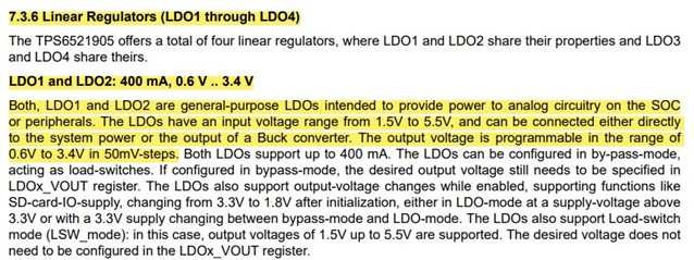
* VLDO1: Use 3.3V output
* Use of DUT Power ON/OFF KEY
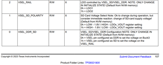
* VSEL_SD/VSEL_DDR: Active "H"

PMIC_TPS6521905_schematics.pdf

Please check. Thank you.

  • Hi Grady,

    For LDO1, you can use a 3.3V input if you use this rail as a load switch. Otherwise you will need to raise the input to account for the LDO drop-out voltage.

    The Push Button configuration looks correct in order to implement a Power ON/OFF key. Push Button can be held low for the selected deglitch time after VSYS crosses above UVLLO threshold to start the power up sequence (make sure Fist Supply Detection is disabled to avoid power up as soon as UVLO is crossed). Be sure to set this pin as Push Button Configuration in R20 bit [5:4] (MFP_2_CONFIG register).

    VSEL_SD active high configuration looks good. MFP_1_CONFIG register bit [1] should be set to 1b so that HIGH signal on this pin causes LDO1 or LDO2 (depends on configurations settings) to be 1.8V output.

    Or, if you want LDO1 / 2 to follow the LDOx_VOUT setting, you should set MFP_1_CONFIG bit [1] to 0b according to your current pin strapping.

    Regards,

    James

  • Hi, James

    Thank you for response.

    Customer have additional question.

    Since the above answer only covers the use of BYPASS and LOAD S/W, I would like to ask you additional questions.

    The datasheet of TPS6521905 indicates that the output voltage of LDO1/2 can be programmed in 50mV steps within the range of 0.6V to 3.4V.

    Q1) Is it possible to program the output voltage of VLDO1 and VLDO2 by inputting VSYS (4.2V) to PVIN_LDO1 and PVIN_LDO2 applied to the circuit? Is it impossible?

    Please check. Thank you.

  • Hi Grady,

    Can you clarify the question? I'm not sure I understand.

    The programming of the LDO1/2 outputs is determined by the register settings. You will need to apply a high enough voltage to the PVINx inputs to account for the LDO dropout.

    There's not way to program the output voltage based on the PVINx input.

    Regards,

    James