This thread has been locked.

If you have a related question, please click the "Ask a related question" button in the top right corner. The newly created question will be automatically linked to this question.

LM25148: Load dependent instability

Part Number: LM25148
Other Parts Discussed in Thread: LM5148

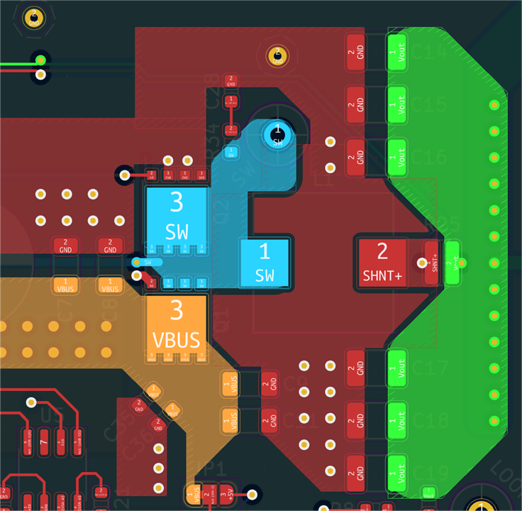
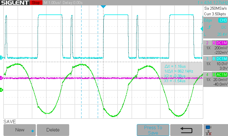
I am developing a power converter based on the LM25148. I made a post here two weeks ago about stubborn instability. That thread found I had not followed all layout guidelines for the chip, so I went back to the design and re-fabbed the boards. Unfortunately, the behavior did not go away and in some ways has become worse.  The main symptom is oscillation of the output voltage and inconsistent switching pulse width. The shot below shows the SW node in blue, inductor current in pink, and output voltage in green. 

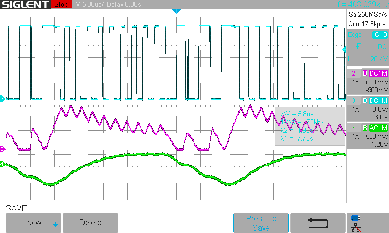
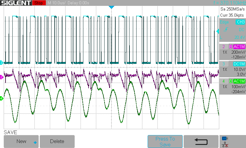
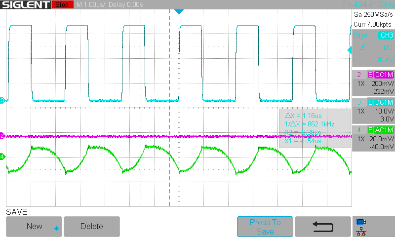
At low loads the converter operates as expected, there seems to be no problem while the converter is in DCM (maybe this isn't the right term since I've enabled FPWM, but it works fine when the average inductor current is less than half of the ripple current). Then it oscillates as shown above, for me between a load of 700mA and 3.5A. Once the load increases above 3.5A it returns to stable operation as shown below. 


Forum_mar5_design_calcs.xlsm

I have attached my design calculator for reference. Assuming I had a subharmonic oscillation or noise problem I have tried to systematically eliminate possible causes. The thing I have tried the most is adjusting the compensation network. I have tried higher crossover frequencies, lower crossover frequencies, higher phase and gain margins, recalculating with different output filter assumptions, and just blind component adjustments. Some configurations are definitely worse; leading to completely useless output, but most of the calculated values give indistinguishable results. 

One additional observation is that the instability exhibits some sort of hysteresis. When the load is reduced to nothing from 4A, the no-load state is no longer operating as expected.

This is fixed by power cycling the device, which causes it to return to normal. 

Since I could not adjust the compensation values to fix this problem, I tried adjusting many other things. 

I adjusted the output filter, using 2.2uH, 4.7uH, 6.8uH, 8.2uH, and 10uH. None of them altered the behavior significantly besides changing what load ranges were stable. Lower value inductors had higher ripple current and stayed stable at a larger range of low currents. 

I removed my feedback network and tied FB to VDDA through a 100k resistor, setting the output to a fixed 12v. This did not change the behavior and I believe eliminates the possibility of noise on my FB network being the culprit. 

I added a few different filters between the ISNS+ and Vout pins close to the LM25148 chip. These had no effect. 

I switched to internal compensation which was worse than all my external attempts. 

Are there relationships I can investigate or nets I can probe that would give insight to this issue? I do not have experience with peak mode current control before this design and I fear I'm missing something.

  • sorry you are still experiencing difficulty Liam,

    Can you share the schematic of your board, another cause for instability is the input filter, I want to check that.

    Thanks.

    David.

  • Hi again David, thanks for your time. Please see the schematic below. If it's of any use I did probe the input voltage multiple times when testing and I did not see excessive ripple or any obvious correlation to the output ripple. You can ignore the current feedback pathway and the digital potentiometer. That's for eventual adjustable current limit functionality and is currently disconnected from the board. 

    Here is the physical implementation of the input filter, I believe I did a good job of minimizing loop area but let me know.

    I can try adding an input inductor to the circuit, should I place it before the entire board or just before the power section?

  • Hello Liam, 

    It's not so much about adding a filter, more to do with damping fo the input.  I see you have a C6 installed, what's its ESR Value.  Note: even though you do not have a filter, you may still require damping if you are using long inductive cables to the input of your board.  C6 with 100mR's of ESRshould provide adequate damping and rule this out of our investigation.

    I noticed a lot of additional circuitry to the input pins of the LM5148, suggest depopulating these to ensure these subcircuits are not interacting with the loop.

    Hope this helps.

    David.

  • Hi David, 

    The electrolytic I have installed does not have an ESR specified by the manufacturer, but it is a quality Panasonic part #ECA-1HM331B. I could whip up a test jig to analytically measure the ESR but I could also add another in parallel or remove it from the circuit to see if it has an effect. Which process would give you more clarity?

    As far as additional circuitry is concerned, do you mean the opamps? R24 is unpopulated and I have disconnected the FB net and tied FB to VDDA through a 100k resistor. So none of them are connected to the controller. I can completely unpower U2 to be sure. U3, U4, and U5 are not connected to the controller at all, though I guess U3 could have a small effect on the current sensing, I can disconnect that but that will remove my ability to scope inductor current. I would have expected adding the ISNS filter to have some effect if these nets were the problem. The only other thing I can think that is additional circuitry is D1, which i saw recommended in another discussion about this chip.

    If you have specific components you would like me to eliminate I'm happy to give it a shot but I don't think there's much excess connected right now. 

  • Just to add some more information, I just tried adding an input inductor of 4.7uH to the input voltage before the power stage. I know you didn't ask for that but It's something I hadn't tried. It didn't change the performance at all. 

  • Here's a scope shot of the input voltage measured using tip and barrel technique right across the input capacitor closest to the FETs. It correlates to the switching as you'd expect but doesn't seem too excessive or related to the output ripple. In this shot blue is SW, pink in Vin, and green is Vout. 


  • Hello Liam,

    The potential problem is the OP amps going back the FB node are distancing the FB resistors aways from the FB pin.  did you try to populate the CHF 150pF compensation capacitor?  

    If the 150pF CHF cap does not help, I would try kludging the FB resistors right by the IC and see if that helps?

    If not, can you report how you are routing the current sense traces back the device?

    Thanks.

    David.

  • Hi David, 

    As mentioned earlier, I've completely disconnected the FB network from the device. I've cut the trace and soldered a 100k resistor between FB and VDDA to set a fixed 12V output. This did not change the performance at all. To be sure I completely disconnected the opamp from the board and that also did nothing. 

    Adding the 150pF capacitor was one of the compensation adjustments I tried before, along with putting higher values in that footprint. For completeness sake I just tried again and it still had no effect.  

    See the current sense routing below. The tracks are tightly coupled to each other and have two distinct sections. The first section begins right under the sense resistor and is sandwiched between two unbroken ground planes until the tracks are clear of the switching area. The tracks then come up to the top layer and run over an unbroken ground plane on the layer below. They go through a filter right before the controller. I started with no filter and then tried many cutoff frequencies down to 1MHz. None of the filters changed the behavior. 

    I also depopulated U3 just incase that input impedance was effecting something. This also had no effect.

    This question might be out of scope but is there any way to get on the phone with an Application Engineer at TI? All the TI web pages imply that all the technical support has moved to this forum. We were hoping to have 5k of these in production by now, if we can't get this design basically working by the end of the week we're going to have to abandon this design and order more of a previous design using a different brand of controller. 

  • hello Liam,

    email me at david.baba@ti.com.  Thanks.  David.

  • My issue was resolved by reducing the source of noise itself, specifically the high side gate drive. I slowed the edge by adding a series drive resistor. Losing some efficiency for stability.