This thread has been locked.

If you have a related question, please click the "Ask a related question" button in the top right corner. The newly created question will be automatically linked to this question.

LM5022: LM5022 flyback design-loop compensation

Part Number: LM5022
Other Parts Discussed in Thread: TL431, LM51551, LMV431, LM431

Hi experts,

I have a isolated flyback design with LM5022, the input is 9-60V, output is 12V/2A, transformer turn ratio is 1:1 with Lm=8uH.

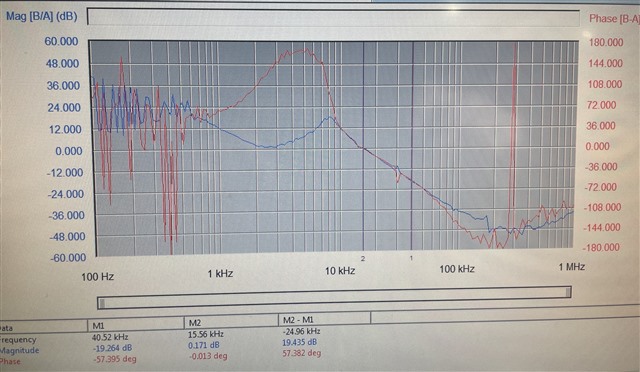
When i tried to measure the bode plot, it gives bad phase/gain margins. Tried to tuned compensation R/C over TL431, but no improvement on bode plot.

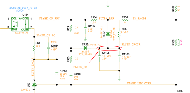
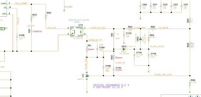
Can you help suggest compensation values for this design? Here is the schematic for reference.

9-60Vin_12Vout-2A_flyback.pdf

Here is bode with 0.2A loading.

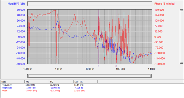
When measure with 2A loading, the bode plot is very noisy as below.
Thanks.

  • Hi Neo,

    I just tried some experiments with the power stage designer.

    Can you try to replace

    R933 ~25k

    C1100 ~ 24nF

    Best regards,

     Stefan

  • Hi Stefan,

    25k/24nF does not work. 

    Instead I changed R61 to 1k or 2k, and R933 to 2.2k, C1100 to 220nF, i got a much improved bode.

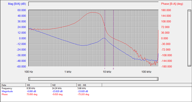
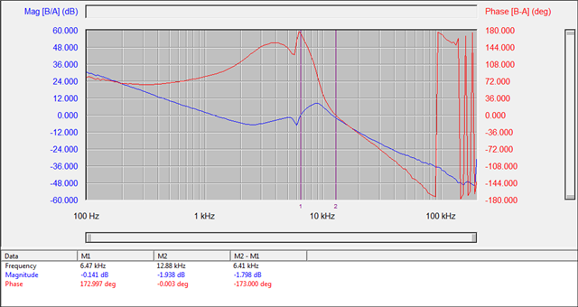
    But in the bode plots, the gain has two times across 0dB, and gain margin is not sufficient. Here are the bode plot at 0.2A and 2A loading.

    Looks like there are two zero @~1khz which boost the phase/gain and then a double pole @~8kHz which pull the phase significantly.

    Can you help me understand which R/C can attributes the double zero and pole? Any idea on how to tune it further?

    0.2A loading


    2A loading.

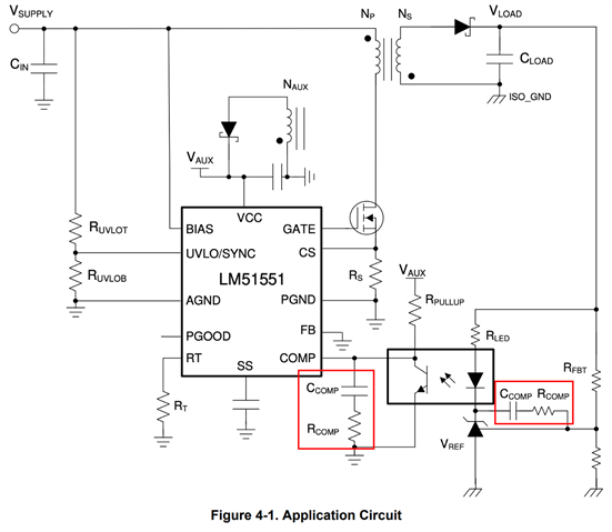
    Also, when I look at TI application note SNVA866A, there are RC connect with COMP pin. What's the purpose for these components? How did they contribute to loop ZERO and POLE? How to choose the value? Thanks.

    Thanks

    Neo

  • HI Neo,

    there is a great report which describes the compensation and how this can be defined:

    Switch-mode power converter compensatin made easy

    Maybe this helps and gives you the required information.

    Best regards,

     Stefan

  • Hi Stefan,

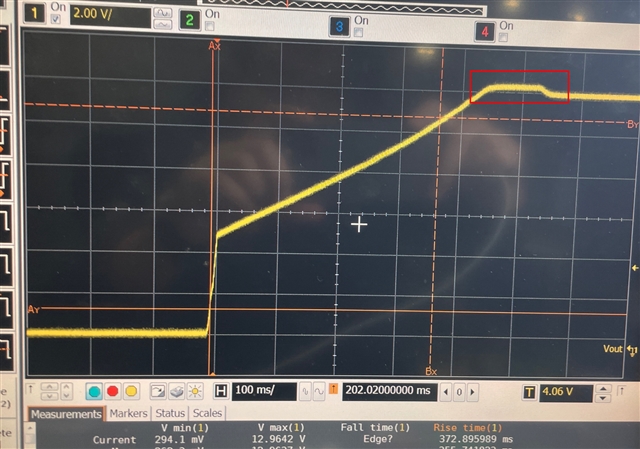
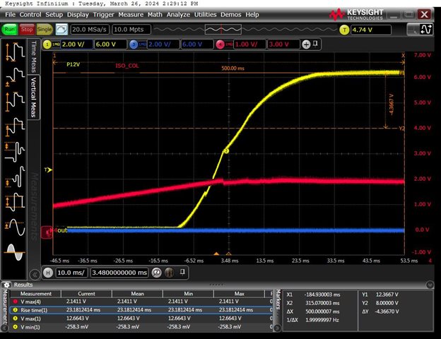
    We probed the startup waveform and shows a voltage step at the end of the ramping up.

    Can you let me know what could cause this? Thanks.

  • Hi Neo,

    did you run this test with load or without load.

    If this is without load the output voltage got overcharged as one Pulse has delivered more energy then the system would consume.
    Can you probe the SW in parallel to see if the controller enters Skip mode for that period or if this looks like an operation mode.

    Best regards,

     Stefan

  • Hi Stefan,

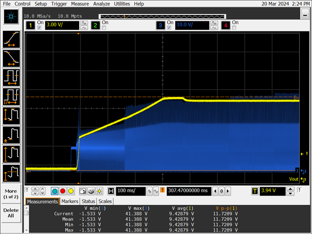
    We run both no load and 2A load, observed the same behavior.

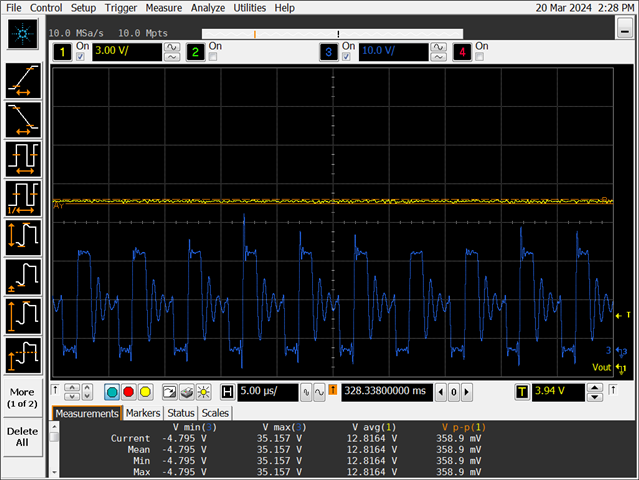
    We probed the SW, no skip mode during that period. Also the time period is about 100ms, so seems not an operation mode.

    Can you help double check? Thanks.

    Startup with 0A load.

    Startup with 0A zoom in.

  • Hi Neo,

    sorry, just realized again that this is a Flyback design.
    I think the issue is in the startup logic which has needs special considerations for a Flyback, please see this document:

    https://www.ti.com/lit/an/snvaa44/snvaa44.pdf

    Best regards,

     Stefan

  • Hi Stefan,

    I did not get any clues why there is a step (about 80ms) from this document.

    Can you give some idea on this? Is it due to too much long ramping up time (about 300ms)?

    Thanks

    Neo

  • Hi Neo,

    as you can see in the datasheet:

    So during the softstart phase the COMP pin gets impacted by the softstart circuit.

    Now the softstart you have on the secondary side (with the voltage regulation) and the softstart block in the LM5022 does both work on the COMP pin.

    So i assume (and you can check) that the softstart charge ramp does also correlate the increase of the output voltage.

    You should be able to avoid this if you make the softstart time at SS pin shorter then the softstart time on the secondary side.

    Note: sorry, i got confused when scrolling up and did see the image of the LM51551 - so I attached the report for the LMN515x softstart.

    Best regards,

     Stefan

  • Hi Stefan,

    Thanks. Per calculation, with SS cap=0.47uF and 10uA charge current, the ramp rate is ~21V/s. While from waveform the ramp rate is ~20V/s, looks like they are matching.

    I will try to reduce SS cap and get back to you. Thanks.

    PS. previous request is to understand the loop compensation with TL431, so snap is from LM51551. Sorry for confusion.

    Neo

  • Hi Stefan,

    I changed SS to 0.1uF, no help. Can you please advise if i should change it to even smaller?

  • Hi Neo,

    can you probe the SS and the secondary side softstart in addition to the output voltage.

    Best regards,

     Stefan

  • Hi Stefan,

    For secondary side softstart, do you mean this node?

    Thanks

    Neo

  • HI Neo,

    yes, this is the part responsible for the Softstart on the secondary side.

    Best regards,

     Stefan

  • Hi Stefan,

    Can you please help me understand the SS behavior of LM5022?

    1. After secondary soft start takes control (opto Diode conducts), will SS cap still be charged? If yes, how much voltage can be charged over SS cap? Any voltage clamping?

    2. With secondary soft start implemented, if SS is keeping charged up, will the SS voltage still impact the COMP pin? If yes, how does it impact?

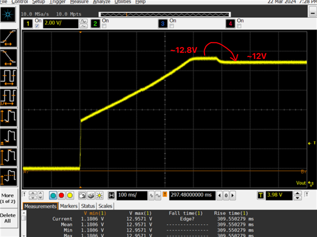
    In our design the set point is 12.8V, so looks like the voltage was soft started but dragged to ~12V by something.

    Thanks

    Neo

  • Hi Neo,

    thanks for highlighting that the target voltage should be 12.8V - was assuming that the 12V should be the target voltage.

    Can you please probe and share the scope plots of output voltage (as shown avobe) on first channel and on second channel:

    - SS of LM5022

    - C1105

    - U13 Pin1 (LMV431)

    - COMP pin of LM5022

    Please confirm that None in above schematic means not assembled or clarify what None stands for.

    Best regards,

     Stefan

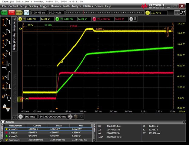
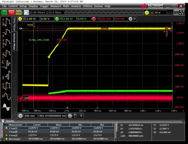
  • Hi Stefan,

    Please find below waveforms. NONE in schematic means the component is not assembled/stuffed.

    1. CH1-12V, CH2- C1105, CH4-SS

    2. CH1-12V, CH2- U13 pin1, CH4-COMP

    Something observed:

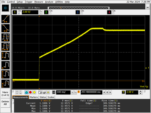
    1. When soldering probe (coax cable) over U13 pin1 (probe across pin1 and 3), the voltage drop disappeared and ramps up smoothly to a stable 12.8V. See above waveform in #2.  After removing the coax cable from U13 pin1 and 3, then the voltage drop appears again.

    2. COMP voltage is pretty low, close to 0V, but still we observed the switching didt waveform and Vout ramps up. Measured U114 pin 4-3 with DMM, voltage gives ~0V. Confirmed it's not probe issue.

    Can you please share your thought on this?

    BTW, on this board during testing, a few BOM has been tuned to have good phase margin. Here is the BOM value changes for your reference.

    Thanks

    Neo

  • Hi Neo,

    thanks for the update.

    So it looks like some disturbance is getting injected on to the FB/REF input of the LMV431 but this should not be a loop stability issue.

    This issue could be due to:

    - LMV431 being placed very close or below the inductor - can you please check and let me know

    - common mode filter not placed or damaged - can you please confirm R929, C1096, C1097, C30, C1098 are placed and esp. R929 is not damaged or broken

    - layout of LMV431 REF is done properly with avoiding noise pickup

    - layout of LM5022 COMP is done properly with avoiding noise pickup

    Some other countermeasures you can try:

    - adding a filter Cap for HF noise to COMP (COMP to GND) e.g. with 1nF can help 

    - adding R29 with 1k can help if the LMV431 will not get enough current for operation

    -> can you please check the above items and and let me know

    Best regards,

     Stefan

  • Hi Stefan,

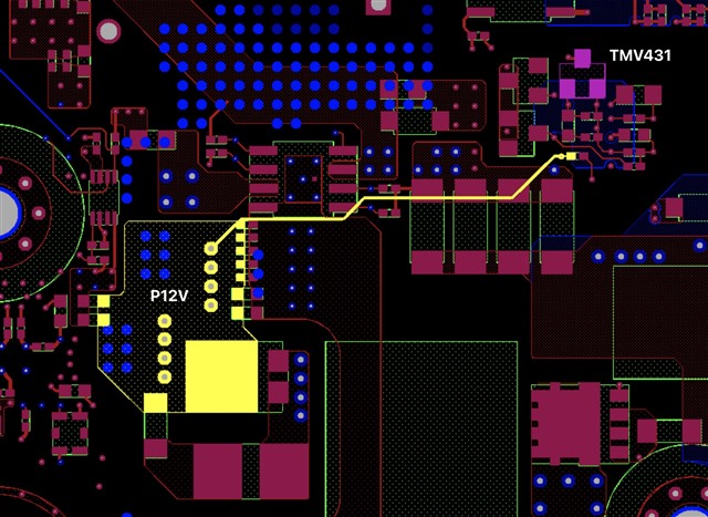
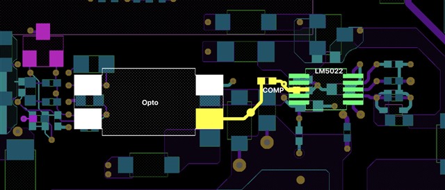
    1. LMV431 is away from switching parts in layout, see below snapshot.

    2. We can probe SS and DIDT voltage with reference to ISO_AGND, so R929 should not be damaged.

    3. Please refer point#1 where the yellow trace is routed from Flyback output to TMV431 section for voltage sensing.

    4. COMP is a short traces between LM5022 and Opto, away from noising source.

    Questions:

    1. If the TMV431 operation current is not enough, the COMP should be close to 5V, instead of 0V, right? As per datasheet, the operation current is pretty low, so i assume the no R29 is needed. Please correct me if i am wrong.


    2. Why soldering a coax cable probe to TMV431 pin1 and 3 solves this issue? From my understand, a very small capacitance can be added after soldering the coax cable. Can i add a small cap like 10pF over TMV431 pin1-pin3? If yes, will this cap affect the loop stability?

    3. Basically do you see any issue with COMP close to 0V? If this is true, there should be no output and DIDT pulse, right? 

    4. To add a cap between COMP to GND, do you mean 1nF cap over Opto Pin4 and pin3?

    Thanks

    Neo

  • Update:

    1. adding R29 with 1kohm, no help, and observed output voltage slightly higher (starts up to 13V then drops to ~12.6V).

    2. adding 1nF on COMP to GND, no help.

    3. adding 10pF in parallel with R939, no help.

    4. R929 is good, and also the impedance between C1097 is 2kohm.

  • Update: We changed C1105 to a 4.7uF cap and removed C1106 from board, voltage ramps up smoothly but stable at 12.4V. Our design target is 12.8V.

    Measured U13 pin1, its 1.232V instead of 1.24V. 

    Can you help advise what could cause the voltage inaccurate?

    CH1-12Vout, CH4-COMP

    Thanks.

  • Hi Neo,

    there still seems to be some noise injected into the VREF of the LM431 (Note you mentioned TMV431 several times before but this should be LMV431 -right?)

    Would be good to find the route cause of this noise but if not adding a small cap to VREF can also work.

    It should not impact the loop if this is just a few pF but please check the loop again with a bode plot.

    Best regards,

     Stefan

  • Hi Stefan,

    I put 10pF across Vref and GND, no help, should a higher value put like 100pF?

    As updated earlier, by changing secondary soft start cap from 2x47uF to 1x4.7uF, voltage ramp up is smooth, but still slightly lower than target output voltage.

    Yes that's a typo, it should be LMV431 which is used in my design.

    Thanks.

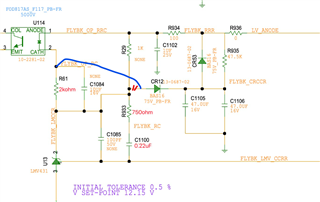
  • Hi Neo,

    just out of curiosity can you try out this modification:

    connect CR12 Anode to U114 pin 2 directly.

    Best regards,

     Stefan

  • Hi Stefan,

    What's the purpose to for this connection? Do we need to cut the trace of red marked area?

    BTW, we tried a few changes and here are the findings:

    1. Change C1105, C1106 2x47uF to a 4.7uF cap, voltage can ramps up smoothly but slightly lower (12.4V) than targeted 12.8V.

    2. Keep C1105 =47uF, remove C1106, and change R61 from 2kohm to 1kohm, voltage ramps up smoothly with expected voltage 12.8V.

    Why R61 impact the output voltage?

    Thanks

    Neo

  • Hi Neo,

    I would not cut the trace on the PCB but either rotate or lift up CR12 so that it das not contact on the anode side and then blue wire.

    I would like to checkout if the diode (e.g. with its reverse recovery charge) and the Softstart caps C1105 and C1106 will have some impact on the loop control with the LM431 esp. if this is connected after the R61.

    Esp. as you now have also seen that changing R61 and also the SS caps have some impact on that issue.

    Best regards,

     Stefan