Other Parts Discussed in Thread: LM5069, LM5066
Hello TI,
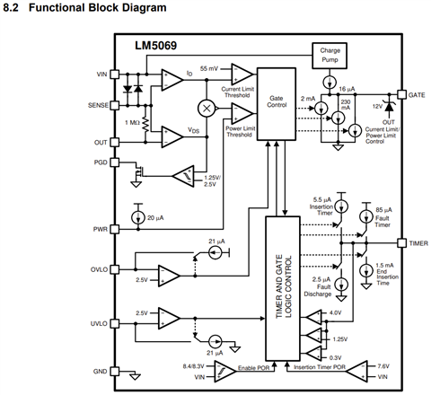
I have two equivalent designs using LM5066 and LM5069. While testing for reverse input voltage behaviour, I discovered that these 2 parts have internal diode voltage when measured from GND to each pin. However, the internal diodes are not illustrated in the component block diagram.
Can you help to confirm the presence of the internal diode, its type and purpose?
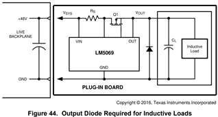
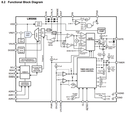
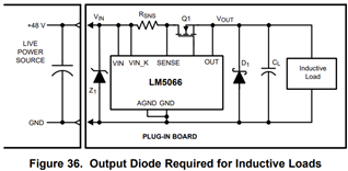
LM5066 and LM5069 datasheet recommends output schottky diode for inductive loads, but only LM5066 datasheet suggests zener diode at the input (Figure 36)
LM5066
Measurements taken on LM5066 component removed from PCB
| Pin # | Pin | GND-Pin (V) | Pin # | Pin | GND-Pin (V) |
| 1 | OUT | 0.679 | 15 | VREF | 0.569 |
| 2 | GATE | 0.616 | 16 | DIODE | 0.574 |
| 3 | SENSE | 0.630 | 17 | VAUX | 0.574 |
| 4 | VIN_K | 0.604 | 18 | ADR2 | 0.573 |
| 5 | VIN | 0.604 | 19 | ADR1 | 0.574 |
| 6 | NC | OL | 20 | ADR0 | 0.574 |
| 7 | UVLO/EN | 0.668 | 21 | VDD | 0.498 |
| 8 | OVLO | 0.165 | 22 | CL | 0.618 |
| 9 | AGND | 0.000 | 23 | FB | 0.680 |
| 10 | GND | 0.000 | 24 | RETRY~ | 0.661 |
| 11 | SDAI | 0.572 | 25 | TIMER | 0.616 |
| 12 | SDAO | 0.572 | 26 | PWR | 0.608 |
| 13 | SCL | 0.574 | 27 | NC | OL |
| 14 | SMBA~ | 0.757 | 28 | PGD | 0.637 |
LM5069
Measurements taken on LM5066 component removed from PCB
| Pin # | Pin | GND-Pin (V) |
| 1 | SENSE | 0.711 |
| 2 | VIN | 0.608 |
| 3 | UVLO | 0.675 |
| 4 | OVLO | 0.661 |
| 5 | GND | 0.000 |
| 6 | TIMER | 0.658 |
| 7 | PWR | 0.650 |
| 8 | PGD | 0.635 |
| 9 | OUT | 0.685 |
| 10 | GATE | 0.612 |