


Nice to meet you. I am writing this because I want to know about the Gate Driver Desaturation Protection Flow.
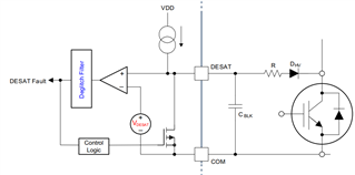
From what I understand, firstly in the Normal Operating situation, IGBT turns on -> Vce goes low -> DHV turns on -> the internal current source does not get delivered to Cblank but flows through the upper path (resistor and diode), so Cblank does not get charged enough(under Vdesat).
--> The voltage of the Desat Pin is expected to be Vce + 0.7V.
And in the Short Circuit situation, Vce goes high -> DHV is turned on, so the Desat Pin voltage increases (Vce + 0.7V) -> When the Desat Pin voltage reaches Vdesat, the FLT signal is output.
I would appreciate it if you could let me know if there are any errors or points to be corrected in the Signal Flow I understood.
