Hi TI
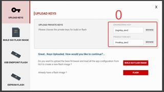
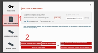
Do I need to burn the latest version of firmware to the IC to support PD3.0?How to quick start TPS25762-Q1?
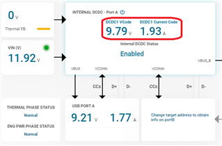
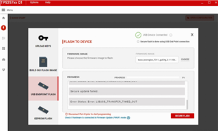
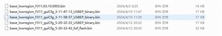
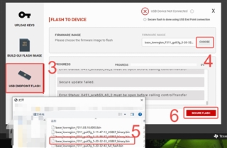
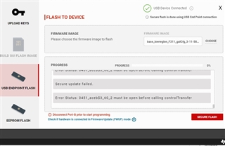
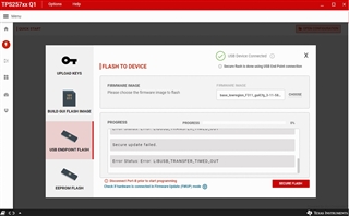
When I burn the firmware,the log show error,what mean of the error?
Thanks~
Hi TI
Do I need to burn the latest version of firmware to the IC to support PD3.0?How to quick start TPS25762-Q1?
When I burn the firmware,the log show error,what mean of the error?
Thanks~