This thread has been locked.

If you have a related question, please click the "Ask a related question" button in the top right corner. The newly created question will be automatically linked to this question.

LM5177: Compensation component selection

Part Number: LM5177

Hi TI,

We use LM5177 as 9~48V DC input regulator. Here are our design parameter.

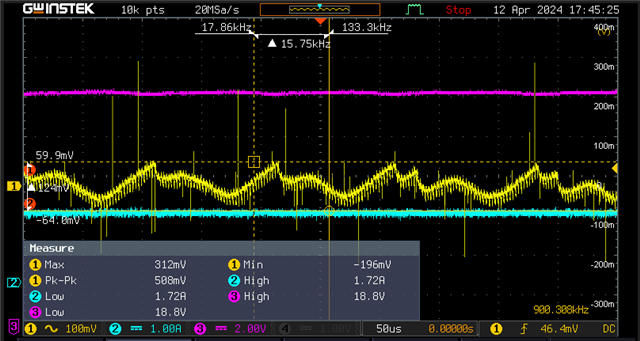
Base on our current setting, we can observe the low frequency ripple.

Are there any suggestions to optimize this low frequency ripple?

If I need to fine tune the compensation components, do you have any guieline to determine the crossover frequency and phase margin?

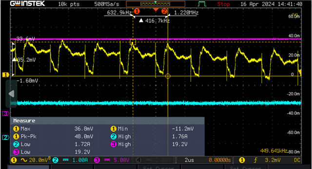
Fig 1. Ripple under 1.75A load
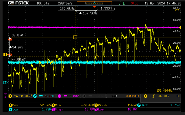
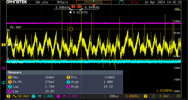
Fig 2. Low frequency Ripple under 1.75A load
AMR_LM5177_20V_3A5_Buck-Boost Quickstart Tool V1_0_9.xlsm

LM5177.pdf

  • Hi Austin,

    thank you for using the E2E forum.

    For the compensation the system needs to be stable on the whole operation range (Vin and load current).

    To have it stable 3 criteria should be considered:

    - Phase margin > 50 Degree - recommended > 60 Degree

    - Gain Margin > 12 dB

    - Gain slope and cross over frequency - 20dB/Decade

    A good approach to define the cross over frequency is:

    - fc < f_SW /10 and fc < f_RHPZ /5 

    For f_RHPZ you should select the lowest input voltage

    In the excel calculator at the value of Vin,min you will get the f_RHPZ of 55kHz, so a f_SW of 10kHz is a good starting point.

    Now set the bode plot to Vin, nom = Vin,min and make the compensation to have a stable system, e.g.:


    Then check if the system is stable over the full operation range and readjust if required.

    Best regards,

     Stefan

  • Hi Stefan

    I check several Vin for fc

    Vin= 9V, fc~4.4KHz, PM~77

    Vin=19V, fc~9.9KHz, PM~78

    Vin =56V, fc~2.3KHz, PM~78

    I think this setting can meet the design guide line

    When I implement this setting to my circuit, I still can observe low frequency at each Vin.

    Is there any suggestion to improve this low frequency ripple?

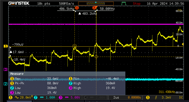
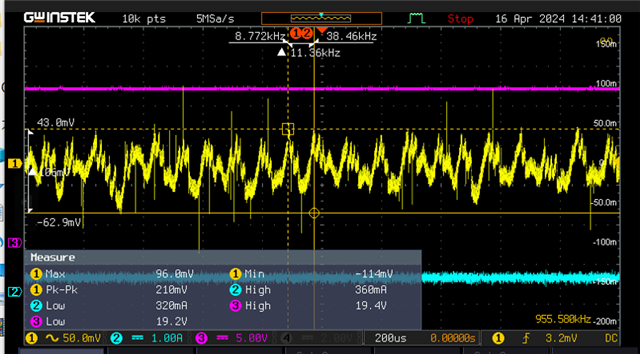
    The waveforms measured on my board are shown below

    I can observe the ripple noise around 10KHz.


    Can this ripple be improved by fine tuning the compensation components?

    CH1: +20P0V_DSW

    CH2: Load current

    CH3: +VCC_DC_IN_CONN

    +VCC_DC_IN_CONN = 19V

    Load current: 350mA

    +VCC_DC_IN_CONN = 19V

    Load current: 1.75A

  • Hi Austin,

    thanks for the update - just realized that the data in the excel sheet did not match your schematic.

    So based on the COMP filter in your schematic the compensation should be OK.

    So it might be also something else in the design. 

    Can you share some scope plots additionally showing the SW1 and SW2 or inductor current.

    When you share the layout, I can review that as well.

    Best regards,

     Stefan

  • Hi, Stefan

    Thanks for your kindly update.

    Could you give me a private link to upload our layout?

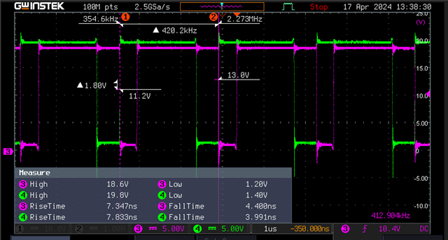
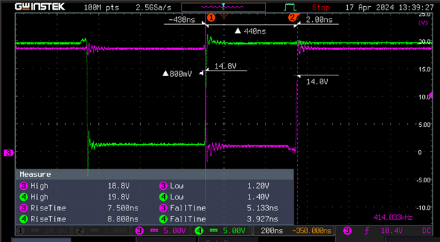
    Besides, here are the waveform for SW1 and SW2

    CH3: SW1

    CH4: SW2

    +VCC_DC_IN_CONN = 19V

    Load current: 1.75A

  • Hi Austin,

    on a quick check the switch node frequency looks stable - may you can check and confirm that this is really the case even over a longer period.

    If you klick on my name you can send me a private message. If done please drop a note here so that i know to check that mailbox.

    Best regards,

     Stefan

  • Dear Stefan

    I send you a private message. Please use  the link to get my layout file.

  • Hi, Stefan

    Did you get my layout file for reviewing?

    If there are any update, please let me know.

  • HI Austin,

    there are some comments on the layout:
    (Checked below items - bold could be improved)

    • Kelvin connection to CS/CSG sense resistor
    • CSA and CSB are surrounded by SW1 or other static signal
      • CSA/CSB  is crossing LDRV2, HRDV2, SW2 , LDRV1 -> noise can couple in 
      • Whole filter should be close to LM5177 (incl, R2128 and R2134
    • Kelvin connection to ISNS+/- sense resistor (shorted to GND if not used)
    • Small current loop for HO1/SW1 (SWx and HOx routed on top of each other)
      • next exact - could be a little bit better
    • Small current loop for HO2/SW2 (SWx and HOx routed on top of each other)
      • next exact - could be a little bit better
    • Feedback connection after or in-between the output cap
    • VCC cap close to Pins 
      • avoid connecting VCC cap with vias
    • AGND ground area/plane used (all AGND based components are place and connected to this area)
    • AGND and PGND connected at Thermal pad

    If something is injecting noise into the AGND and the components referenced to the AGND the regulation can get some disturbance.

    The sensing of the Rcs (CSA/CSB) is the most critical in this circuit. Disturbance injected into this signal can have impact on the regulation.


    Best regards,

     Stefan

  • Hi, Stefan

    Thanks for your comments for my layout design.

    But I can't realize which is the key point about the low frequency ripple.

    Do you have any other idea about this issue?

  • HI Austin,

    You can also try to increase the output cap and make the compensation filter more aggressive by shifting the crossover frequency to 15kHz

    If this does not improve the ripple can you please check the following items (over 2-3 VOUT "Oscillation periods"):

    - stability of VIN

    - COMP Voltage

    - SW1 and SW2 

    - Inductor current

    Do any of this signal change with VOUT?

    Best regards,

     Stefan.