This thread has been locked.

If you have a related question, please click the "Ask a related question" button in the top right corner. The newly created question will be automatically linked to this question.

UCC28951: Testing the UCC28951

Part Number: UCC28951
Other Parts Discussed in Thread: UCC28950

Hi Mike O' / Team,

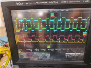
I want to start testing the controller (UCC28951) which is assembled on the PCB. I'm Preparing a Testplan to start Testing. Kindly guide.

I want to Start off With NO LOAD condition, then slowly give Load current in Linear order. 

My Max Load current is around 80A. and Minimum is 2A.

Tmin Resistor: 13K. Should i further reduce Tmin resistor value or is this correct?

In the datasheet section 7.3.9(Burst Mode), It says, If the controller is still demanding a duty cycle less than TMIN, then the controller goes into shut down mode. 

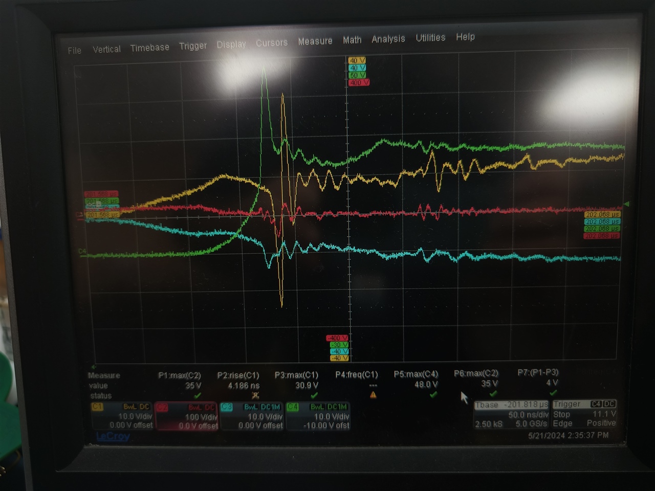
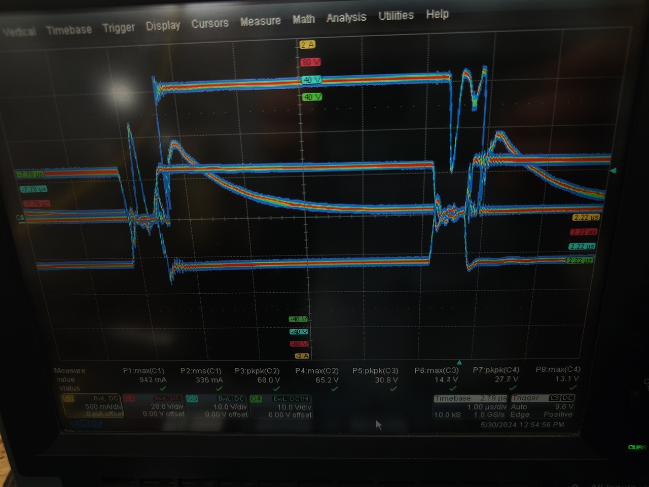
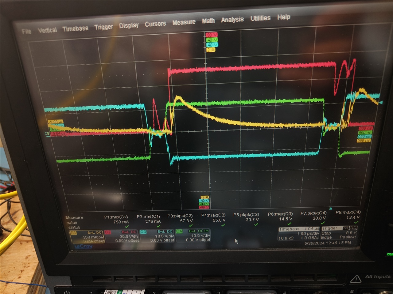
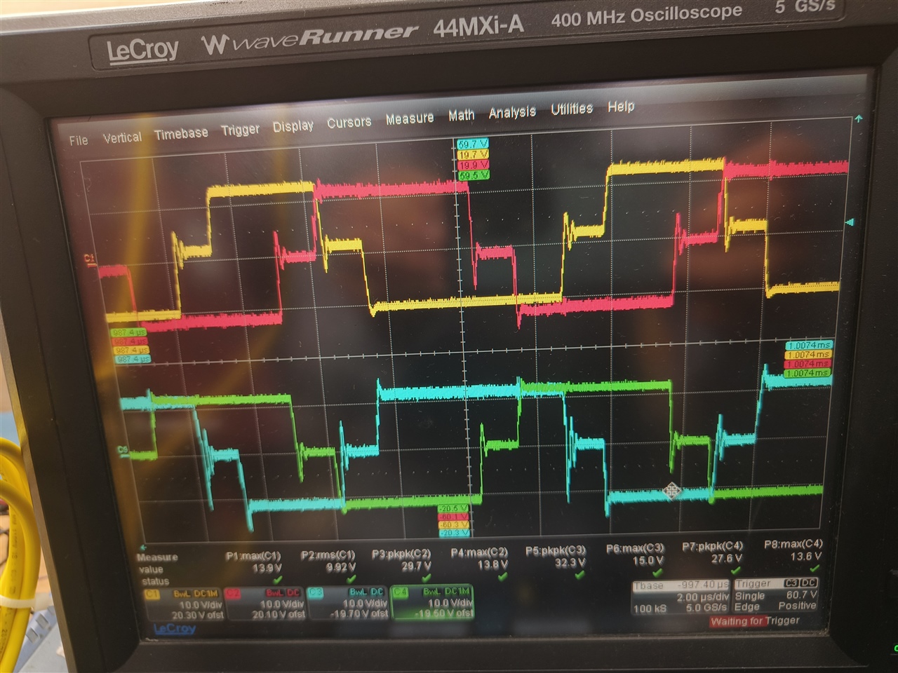
I'm Getting confused with the different modes of operation. As i Understand When the controller starts after SS/EN pin is released, the output voltage should be regulated with No load. 

Then Let's say i give load current of 2A (it will be very light load conditions),

Then let's say I increase the Load current to 5A, it enters DCM mode or still be burst mode?

Further Increasing (Approx 10A in my case) less than 15% of load current which is huge as the FET diodes will heat up, It Will stay in DCM mode. Correct?

More than 15% of load current, The Controller enters CCM mode. I want to understand Whether my understanding of operation is current and what Tweakings / Value changes i may need to do while testing? Please guide.

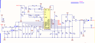
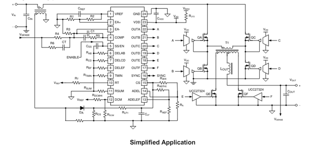
Find the circuit diagram Below.

  • Hello,

    Your inquiry has been received and is under review.

    Regards,

  • Hello,

    When the duty cycle is less than programed by Rtmin the gate drives will terminate but the converter is not in a shut down mode.  When the voltage amplifier output increases to point where the duty cycle is > than what is programed by Rtmin, the gate drives will immediately demand duty cycle.  This is light load bursting.

    There is an over current hiccup mode protection that will instigate a shut down and re soft start.  This is described in section 7.3.14 in the data sheet.

    To protect your FETs from reverse current you should turn them off with the DCM compactor before reverse current can occur.

    The following link will bring you to an application not that goes through the step by step design process using the UCC28951.  There is a link to an excel design tool that goes along with the application note.  These design tools will help you setup the DCM comparator to prevent reverse current in the FETs., 

    https://www.ti.com/lit/pdf/slua560

    In regards to bringing up the design I would recommend the following.

    1. Use DC supply with current limiting to power the design.

    2. Start with 10% resistor load and evaluate stability thermal and critical nodes.

    3. Slowly bring up the load while monitoring critical nodes and stop/troubleshoot/redesign if necessary.

    Regards,

  • Testing the controller now. No DC input supply, Only Bias supply

    Below are observations. 

    Gate drive pulses (OUTA, OUTB, OUTC, OUTD) able to see them.

    What i observed is After some time (maybe 30 40 Seconds later), the controller stops working. When I check voltage at SS pin, it is less than 0.53.

     If I turn OFF the bias supply immediately and turn it ONN, Controller doesn't start.

    But let's say if i turn ONN after some time, it starts working fine for about 20 30 Seconds, and shutsdown again.

    FYR,

  • Hello,

    Your inquiry is being reviewed and I will get back to you shortly.

    Regards,

  • Hello,

    The SS is 0 and outputs stop switching.  The device recovers after letting it sit for awhile.

    Did you check Vref to see if was regulating at the correct voltage?

    You might have lost VDD during this testing and it caused the device to shutoff.

    Regards,

  • Vref is between 5.05V ~ 5.3V. Even though SS pin is less than 0.53, I'm able to read Vref.

    VDD is constant (checked in scope), No dips.

  • Hello,

    If VREF is high that means the IC has power and something has pulled SS low.

    Do you think Q13 is pulling SS low?  I would try disconnecting it from the circuit just to see if it removes the issu.

    Regards,

  • I had similar doubts, so I disconnected R74, R76, placed 820K across SS capacitor to make it like a standalone device. Still SS shows low. Randomly Controller is turning ON, like one in 20 times. Sometimes if leave device turned OFF for longer time, then it's turning ON. Random behaviour. 

  • Hello,

    If the device is running in follower mode the design  needs an 820 k ohm resistor to ground.  Otherwise the device could enter a test mode.

    How about tying the gate of Q13 gate to ground and using the 820 kohm resistor on the SS pin and retesting.

    Regards,

  • Q13 is removed, controller Video gameis working.

    Will try fixing Q13 at later stage.

    Couple of other issues.

    Burnt Qc QD, And synchronous FETs @ Vin 250V. So starting to debug and changing Vin slowly now.

    Now, controller is turned ON, set input to 22V, synchronous FETs are in diode mode. below are observations:

    1. Waveforms at drains of Qc, QD. There is that burst type of outputs, which was not observed on QA, Qb leg. Is that how it's supposed to operate??

    2. Below is the peak observed at drains @Vin : 20V

    Also there was some noise starting which I suppose should be switching noise.

    Yellow is the output regulating to 2V. Is that peak as expected? How to avoid ?

    3. Measuring CT input current, seems to be lot of noisy output. I suspect measurements error using a lengthy wire, also arevthere any additional reasons I should be careful here ?

    Red colour waveform. 

    Additionally guide me whether I'm going in right direction or are there any additional things to be taken care of ?? Based on your inputs I will work on changes Tomo. Thanks

  • Hello,

    Your inquiry has been received and is under review.

    Regards,

  • Hello, 

    The drain of QB and the drain of QC are the switch nodes across the H Bridge.  I would expect the peak voltage would remain unchanged.  In your evaluation the first waveform shows the peaks are changing.  This is most likely due to the input voltage dropping out.  So you DC supply is most likely current limiting to protect the design.

    In regards to your waveforms you mention the waveforms of QC and QD drain.  These waveforms do not look correct for what FETs QC and QD drains and the voltage is at the incorrect level.  Please refer to the simplified schematic of the phase shifted full bridge using the UCC28951.  Could you tell me which FETs these waveforms came from based on the block diagram below?

    I am thinking that maybe the scope plots that you have taken are from the SR FETs drains.  If they are they do not look correct either.  They should not be changing frequency.  There might be something wrong with the way you are driving your FETs.  You may want to double check the connections vs the simplified schematic and application not slue560 to make sure you are controlling the correct FETs with the correct output.

    https://www.ti.com/lit/pdf/slua560

    Regards,

  • 1. The thing which I noticed about synchronous FETs as per 600W design is , when transformer winding 1-3 is on positive side, Q5 is OFF, Q6 is ONN. 

    Yellow: Q5 drain to source

    Red : Q6 drain to source

    Blue : transformer pin 1 ( positive probe ), pin 3 ( negative probe )

    So When Qa to QD is ONN, outF should be ONN.

    Qc to Qb is ONN, outE must be ONN.Verify and  Confirm from your end??

    Does the synchronisation  direction should match  with transformer postive and negative or we can just connect outE and outF random??

    2. The unwanted behaviour observed yesterday is due to the fact that I have connected two different FETs on the Qc, QD ( gate charge : 390nC ) leg w.r.t. QA,Qb leg,  which has ( gate charge of around 53nC) . Now all FETs are same ( 53nC )

    The switching speeds were not able to make up with the necessary gate charge and gate driver was heating heavily, further continuing costed me the controller today. I varied gate resistor and checked, it's not heating for some time and then it starts heating again. 

    Also do you have a calculation for calculating current required by gate and transformer? First I want to Fix gate charge waveforms before proceeding further. 

    Transformer P/N: GT04-111-252-A

    Mosfet P/N : IPW65R090CFD7XKSA1

  • Hello,

    Your inquiry has been received and is under review.  I will get back to you shortly.

    Regards,

  • Hello,

    To calculate the current required to drive a FET (Idrive) is based on change in gate charge (dQ) times the FETs switching frequencyu

    Idrive = dQ/dt = dQ*fsw

    Regards,

  • Below are the switching waveforms. 

    I'm observing outD before outA, is this ok ?

    Yellow : OutA

    Blue : outD

    Green : outB

    Red : outC

  • Hello,

    These look like the voltages at the gate of FETs A through D and not the output from the UCC28951 directly.

    If this is the case the waveforms look good.  also note there is not an exibit of the miller plateau which means your design is zero voltage switching.

    Regards,

  • Yes, you're correct, these are gate switching pulses. I have not applied Vin yet. Just wanted to confirm gate voltages before proceeding to apply Vin. 

  • Hello,

    Thanks for letting me know.

    Regards,

  • Have applied Vin: 50V,

    Below are the drain to source voltages of Qa, Qb. I'm seeing huge peaks . Any reason why could this be happening?

    Though diodes are present, why are they not suppressing Peaks? Any suggestions?

    FYI, its No Load, synchronous rectifiers are in diode mode.

    Mosfet p/N: IPW65R090CFD7XKSA1

    Diodes: GD02MPS12E

  • Hello,

    You might want to study the gate drive of the FETs along with the drain voltage while this is happening.

    You also might be just picking up stray noise from your scope probe grounding.

    I would try looking at this tip and barrel across the drain to source of the FET to see if things improve.

    You also might want to use a ferrite toroid to form a common mode choke on the scope probe wires.

    I believe there is instruction how to do this in the EVM users guide.

    https://www.ti.com/lit/pdf/sluu421

    Regards, 

  • Ok. I understand and I will implement the same. I want to understand the huge peaks, can we reduce them or is there a strategy to work on ?

    Is the gate drive transformer adding more slew rate in switching  ? Should I check using gate driver ? Please guide. 

  • Hello,

    You need to verify the gates of your FETs are driven correctly.  You also need to determine that you are not picking up stray noise on your scope as previously discussed.  After than take a looks at these waveforms again and we continue the debug process.

    Regards,

  • I tried connecting EVM and capturing gate to source and drain to source waveforms of C and D. No spikes in EVM. Same probe and scope connected in my design, drain to source voltage peak is 5 times is high with ringing. 

    Any suggestions how to continue further? Just stuck there since past week. Any thing to do with Coss Of Mosfets or body diode or synchronous FETs ( presently in diode mode ), how do I proceed further?? 

    Is it a good idea to add some RC snubber across Mosfets to reduce the spikes ? Will it have any impact ??

    At present I have shorted shim inductor as the drain source peaks were high, should I remove freewheel diodes ? 

  • Hello,

    I am reviewing your inquiry and will get back to you shortly.

    Regards,

  • Hello,

    You might want to compare the EVM schematic to your designs schematic and see if there are any differences?

    If you are using a shim inductor make sure that you are using the clamping diodes between the shim inductor and the primary of the transformer.

    This gives a place for the difference in the shim inductor and reflected output current when you come out of freewheeling.

    If you don't have these diodes it will cause excessive ringing on the secondary.

    If you have not schematic issues it may be your layout.  The UCC28951 gives some layout recommendations.  You can also use the EVM to check against your layout.  Remember every inch of trace is roughly 10 nH of inductance.  If you have long traces this will cause excessive inductance that will ring with parasitic capacitance.

    One last thing.  Make sure you turn off your SRs before critical conduction.  If you do not you will develop a negative current in the FETs.  When you turn them off you will have excessive spike that will transfer to the primary.

    Regards,

  • Fyi, Shim inductor is connected along with clamping diodes ( Sic diodes ) 

    SRs are connected in diode mode.

    Vin : 25VDC

    Gate drivers: 15Vdc, controller: 12Vdc

    I tried connecting same film capacitors to the other side of current sense, near to drain of FETs, I don't know whether it's a good idea as per the topology, you can comment on this. The capacitance is ( 75nF || 0.5uF || 22uF ). What happens is gate waveform of D has become much better, but gate of C has ringing and dip near Miller region which in turn effects it's drain to source voltage. 

    Additionally The spikes of drain to source of C is very high. 

    Is the ZVS not Kicking In ? Should I add series capacitor between shim inductor and transformer ? Please suggest. 

    Refer below image:

    Yellow: C gate

    Blue : D gate

    Red: drain source of C

    Green : drain source of D

    Gate waveform of C with dip shown below: 

    Yellow : gate of C

    Green : drain to source of D

  • Hello,

    Your inquiry has been received and is under review.

    Regards,

  • Hello,

    If your gates to your FETs are ringing have you tried adding a resistor in series with the gate drive and the gate of the FET?  This should help with damping the ringing of the FETs at the gate drive.

    You have the drain of FET ringing well above the input.  I am not sure how this happens the body should conduct before this happens.  So this does not seem correct or real. 

    I would double check this tip and barrel around directly across the drain and source of FET D.  You also might want to rap the scope probe wire from prop to scope around a ferrite toroid.  This will form a common mode choke and remove common mode noise from the signal.

    Regards,


  • So the ringing is reduced with some modifications.

    Vin voltage :26V, gate drive transformer voltage: 15V, frequency: 80khz

    1. Using gate drive transformer with 560uH inductance

    2. Using 4.7nF film capacitor across drain to source of each FETs

    3. Gate resistance is around 110ohms

    4. Added diode ( reverse direction) across gate resistor for turn oFF.

    Below is the image of switching nodes ( transformer leads )

    Questions:

    1. Since I have made above changes , lemme know what all changes are acceptable?

    2. Additionally adding external capacitors across drain to source ? Can it be added ? Can I compensate that capacitor discharge with addition of shim inductor? Please advise. As of now shim inductor is not connected

    3. Can I try adding some series capacitor with shim inductor? Will it help in any way ? If yes what values to start with ?

    4. I have added ( 75nF) on the other side of CT transformer, direct to mosfet drain and source. is this acceptable? This is done to reduce huge peaks. Will this disturb the cycle by cycle current sense in the controller??

    Next changes:

    updating frequency to 100kHz

    Reduce gate drive transformer voltage to 12V

    Adding series resistor of around 10ohms to reverse diode

  • Hello,

    Your inquiry is under review and I will get back to you shortly.

    Regards,

  • Hello,

    It seems like you are heading in the right direction.

    Please see my comments below.

    Questions:

    1. Since I have made above changes , lemme know what all changes are acceptable?

    As long as you understand what you changed and why changed it you should be O.K.  However, you should back your design up with reliability and production testing.

    2. Additionally adding external capacitors across drain to source ? Can it be added ? Can I compensate that capacitor discharge with addition of shim inductor? Please advise. As of now shim inductor is not connected

    It is not uncommon to add capacitance from the switch nodes to ground on the primary.  Some designers do this to control the tank frequency.

    If you are trying to dampen ringing you can always add RC snubbers across the FETs.

    3. Can I try adding some series capacitor with shim inductor? Will it help in any way ? If yes what values to start with ?

    You actaully can add RC snubbers across the shim inductor to dampen any ringing. 

    4. I have added ( 75nF) on the other side of CT transformer, direct to mosfet drain and source. is this acceptable? This is done to reduce huge peaks. Will this disturb the cycle by cycle current sense in the controller??

    75 nF is quite large for a capacitor across the CT.  Generally you can reduce the noise from the CT output to the CS pin with an RC low pass filter for the current sense resistor.  Typically designers use 1k to CS and 22 to 220 pF from CS to ground.

    I do have a word of advice.  For every change you make, you should compare a before and after.

    You could have noise on the secondary that is coupling through the transformer to the primary from the secondary.  You can add snubbers across the SRs and/or transformer.

    Lastly you might want to try relaying out your power stage to reduce noise.  Keep you power loops as short as possible.  1 in of trace adds 10 nF of inductance.

    Regards, 

  • Thanks for the inputs.

    I disconnected transformer, it's open circuit just bridge and gate pulses. What I noticed is it's still drawing current From DC source and slowly increasing. I had restricted it 200mA, it was reaching 200mA within some 10 -12 seconds. 

    I removed bottom fets of each leg separately and checked , it's not drawing current. 

    the current drawing is because of shoot through is what I have understood till now.

    FYI, Gate pulses of same leg are opposite in direction. SO GATE PULSES are Ok. A & D switch together, B & C switch together. 

    Layout wise I don't see any issue as such.

    Any idea what could be the reason ? 

  • Hello,

    C and D are phase shifted.  I would double check to see if there is any over lap making the design draw current.

    Regards,

  • Gate waveforms are phase shifted as per the design. 

  • I disconnected the full bridge. Connecting only one half bridge and checking. Soldered Mosfets outside of the board on a bread board. Though I restricted the current to 0.7A, it was still drawing current approx 0.65A . I suspect there is still some shoot through current. I read in the forum that CT helps prevents shoot- through? How it helps ? Anything I need to check with CT, Rtmin or any other variable??

  • Hi Mike,

    1. In datasheet, it says DCM must be used to prevent reverse currents. Should I lift the pin of inductor and monitor the exact current whether it's going to Zero or not ? Is that's what mentioned there or is it something else. Because I also read that The SR drives won’t activate until the load current is high enough to bring the DCM pin above the DCM threshold. Please guide in simple steps. 

    2. For synchronous rectifiers, outE waveform comes first or outF ? As I understand I need to sync it with outA pulse. Is that correct ?

    3. CS pin has some parasitic switching noise? Is low pass filter a way to go ? What's the best tuning for these RC filters near to CS pin so that it filters out these parasitic switching noise.

    4. I also read in one of the debugging document, it says,

    Once operation at a very low input voltage is confirmed then increase the input voltage in steps until Vout is at about 50% of its setpoint. Then increase the load current to about 25% of its full load value. At this point you should check that the OUTE and OUTF gate drives are active and correct. Check the waveforms across the output rectifiers.

    Vout is 50%, means I should regulate to 6V and increase load currents? Please explain and guide. 

    5. Additionally, I have 2 secondaries in transformer as you know, one side which is connected to controller common ground is being regulated at 12.15V, even with Vin upto 400V.

    the other secondary voltage keeps increasing with Input voltage.

    Eg: Vin:130V, Vout : 13.8V

    Vin :200V, Vout :15V

    Any idea what could be the reason?

    FYI, Secondaries connected in series. Feedback is taken from bottom secondary winding sharing same ground as controller ground. Anything to do with feedback?? Both Secondaries FETs are in diode mode. 

  • Khan,

    We will get back to you soon. 

    Thanks,

    Ning

  • Hello,

    I am reviewing your inquiry and will get back to you shortly.

    Regards,

  • Hello,

    Please see the answers to your questions.

    1. In datasheet, it says DCM must be used to prevent reverse currents. Should I lift the pin of inductor and monitor the exact current whether it's going to Zero or not ? Is that's what mentioned there or is it something else. Because I also read that The SR drives won’t activate until the load current is high enough to bring the DCM pin above the DCM threshold. Please guide in simple steps. 

    > You are correct about turning of the SRs to prevent reverse current in the FETs.

    >The following link will bring you to an application note that goes through the step by step design process of a phase shifted full bridge.  There is a section in there on how to setup the DCM comparator.

    https://www.ti.com/lit/pdf/slua560

    2. For synchronous rectifiers, outE waveform comes first or outF ? As I understand I need to sync it with outA pulse. Is that correct ?

    >The controller will synchronize these for you.  The following application note has a section showing how to connect these outputs and set DELEF with respect to A and B.

    3. CS pin has some parasitic switching noise? Is low pass filter a way to go ? What's the best tuning for these RC filters near to CS pin so that it filters out these parasitic switching noise.

    >It is o.k. to use a low pass RC fillter for the CS pin.  Just do not over filter the CS signal and set the pole frequency to roughly 10X the switching frequency.

    4. I also read in one of the debugging document, it says,

    Once operation at a very low input voltage is confirmed then increase the input voltage in steps until Vout is at about 50% of its setpoint. Then increase the load current to about 25% of its full load value. At this point you should check that the OUTE and OUTF gate drives are active and correct. Check the waveforms across the output rectifiers.

    Vout is 50%, means I should regulate to 6V and increase load currents? Please explain and guide. 

    > These recommendations do not seem correct.

    > I would start by load the design with a resistive load at 10% with the typical input voltage.

    > At the 10% load adjust the DELAB and DELCD to get valley switching per application SLUa560.  At this point check the DELEF timing as well.

    https://www.ti.com/lit/pdf/slua560

    >Once you are operating at 10% load gradually increase the output power, while monitoring CS, the switch node and thermals and gradually bring up the power in 10% increments.  If the design is getting hot or thinks seem to be electrically overstressed any time during the process, stop increasing the load and reevaluate/trouble shoot the design and correct any issues.

    5. Additionally, I have 2 secondaries in transformer as you know, one side which is connected to controller common ground is being regulated at 12.15V, even with Vin upto 400V.

    the other secondary voltage keeps increasing with Input voltage.

    Eg: Vin:130V, Vout : 13.8V

    Vin :200V, Vout :15V

    >If you have two secondary windings and one primary the input voltages should be the same.

    Regards,

  • Ok understood.

    1. First as I understand, I will rearrange FETs from diode mode to normal FET.

    2. I have to give a load current of 5A , evaluate valley switching on primary side. 

    DELAB, DELCD : 30K

    DELEF: 70K

    What configuration should I set ADEL, ADELEF PIN ? Shall I configure it now or later ? For now can I connect it to Vref / ground?

    3. Additionally, DCM comprator is set to same values as in EVal board, as I understand for 5A ( 10% of load ), it will still be in DCM mode, I will monitor VDS on secondary FETs? 

    4. Next for higher load currents ( let's say 10A ) , as I Understand, it will move to CCM Mode.

    I need to prove valley switching on primary side . Any difference in waveforms on secondary when it changes from DCM Mode to CCM Mode ? What all I need to probe in scope on secondary side ? Please guide.

  • Hello,

    I have received your inquiry and will get back to you shortly.

    Regards,

  • Hello,

    The EVM was designed based on application note SLUA560.  The following link will bring you to the application note.  It explains how to setup the ADEL, ADELF, DELAB, DELCB, and  DELEF pins.

    https://www.ti.com/lit/pdf/slua560

    You want the DCM threshold set to the point before the inductor current is at critical conduction.  If your design has 20% inductor ripple current it might be a good idea to set the DCM threshold at 15% load.  This will give the design 5% margin before it would have gone to critical conduction.  This will prevent negative current from going through the FETs.

    The secondary waveforms will be different than the primary.  This is due to how the SRs are driven.  Please refer to figure 8-4 of the data sheet for critical waveforms.

    https://www.ti.com/lit/ds/symlink/ucc28951.pdf

    Regards,

  • Thanks for the inputs. Few queries 

    1. I have seen primary FETS failing particularly C, D, and twice C. Below is the board scenario. 

    The SR FETs were updated to FETs from diode mode. Put back gate resistor, gate to source resistor. 

    DELAB, DELCD :50K

    DELEF: 70K

    When I was slowly varying DC supply around 50VDC, FETs were failing, mostly gate to source was getting damaged, drain to source channel was OK. No shoot through currents observed. 

    Also output side , windings are parallel, output capacitance is around 21000uF. Could there be any impact of secondary side FETs turning on due to huge inrush current and damage FETs. It's a theory I have arrived, you can infer and tell your opinion on this.

    Below is a waveform where I see drain voltage dip for momentarily 

    Blue and green : gate waveforms C, D

    Red : bottom side FET

    Yellow: input current 

    2. Additionally, for VIn :400VDC, input current is limited to 700mA at the source.

    When Vin : 400 VDC, output load current is 2A,  input current is 540mA seen at DC source

    What I observed is Input Voltage dips to 360 and settles back to 400VDC?

    Turns ratio transformer: 9

    Is the current normal ?

    Why the dip in voltage?

    3. When using fixed delay approach, what should I do to adaptive delay pins ? Should they open circuit?

    4. Vin : 200V, DC source current : 270mA, diode mode Fets at output, Load current : 1A, Tmin:12K

    Below are the waveforms. My observation is approx every 52.3 uS , there is negative current which is probed at the primary side of CT, gate pulse width of C and D is also reduced at that instant. Your thoughts on this 

    blue, green : gate waveforms

    Yellow: Primary CT current

    Pink: C drain to source.


    Zoomed version

    5. When i Increased Tmin: 33k,

    Case A; Load current: 1A, DC source current: 220mA

    The previous reverse current peaks visible in Yellow channel were not present. 

    Blue: Gate source of C,

    Green: C gate before pulse transformer

    Pink: Drain source of C

    Yellow: Primar Current CT

    Case B; Load current: 2A, DC source current: 380mA

    The previous reverse current peaks visible in Yellow channel were present, but small. Here Some audible noise started appearing. below is the waveform. Gate drive transformer negative side doesn't look Ok. Your comments.

    Zoomed out Version below

  • Hello,

    Your inquiry has been received and is under review.

    Regards,

  • Hello,

    Could you send me a complete schematic to review?

    Regards and Thanks,

  • Hello Mike.

    Please share your mail id. It's confidential information to share here.

    Additionally I was debugging the board. Below are the observations.

    There was no ON time between D & A. Then I started probing on D waveform tracking in from controller to gate of FET. No issues were observed on the burst mode. All waveforms were 50% duty cycle. 

    When I tried to load it with 1 A -2A current, I was facing this issue. And sometimes D waveform was so small, that it was not at all 50% duty ratio. When I probed further, what I also observed is transformer primary current, I'm able to see that 2mH charge , i.e.  but the other leg, negative side it's not charging, it's dropping very sharp, that shouldn't happened with 2 mH inductance. Then I suspected something at the output, I removed FETs replaced with schottky diodes. Diodes are placed in same direction as MOSFET source to drian diodes. Cathode of both diodes is connected to other two windings.

    still transformer primary side positive is charging, negative side, it's sharp transient. Below waveforms are available for understanding. 

    Yellow: D

    Red : A

    Blue : C

    Green : B

    Also see the below image where transformer and primary CT currents have been captured. There is no negative side current. 

    Green : primary CT

    Yellow: transformer 

    Blue : switch node voltage.

  • Hello,

    I am not sure why you can't share the schematic of a phase shifted full bridge design.  However, if you can't share it on the e2e that is O.K.

    Please use the schematic in application note SLUA560 to compare to see if you have done anything different that what is recommended.

    https://www.ti.com/lit/pdf/slua560

    Please do a self review of your schematic using slua560 and report your findings?

    Regards,

  • Hello Mike. You have already reviewed my schematic snippets in my last post which you have tagged. Time and again I'm telling you it's confidential data. 

    Colin would never ask to post schematics here, he would always ask to share to mail id. 

    I have asked a query in my last reply, could you please respond to thay.

    If you're not willing to assist , rather than just sending back to 600W application note, could you please transfer the query to a different expert ? 

    Also People at At TI, can you look into this issue ?

  • Hello,

    Colin is a good friend and colleague of mine. I know that he would have asked you for a schematic to review.

    If you can't provide one for review, that is O.K.

    I am sorry that you can't post your schematic.  The UCC28951 has been released for years and when setup correctly will protect the FETs from damage.

    The following link will bring you to an application note that you can use to check your design.  There is also an excel design tool inside.

    https://www.ti.com/lit/pdf/slua560

    I do have another suggestion.  You could also review the 600 W reference design that you can find at the following link.  There is a UCC28950 controller in the EVM.  However, the UCC28951 is pin for pin identical and is a replacement for the UCC28951 and has been verified to work in the EVM.  Please note it was design with the information in application note slua560. You can find the user's guide in the following link.  You can review this design and compare it to yours to see what is different.  There are waveforms in the EVM that you can compare to your design.  It may be even worthwhile for you to order the EVM to evaluate.  https://www.ti.com/lit/pdf/sluu421

    There is another option as well.  You might consider using an existing reference design.  The following link will bring you to the reference design library where you can input your power requirements.  The tool will search the data base and suggest the closest reference designs that will work for your application.

    https://www.ti.com/reference-designs/index.html

    Regards,