This thread has been locked.

If you have a related question, please click the "Ask a related question" button in the top right corner. The newly created question will be automatically linked to this question.

UCC28951: Design 1kW supply guide , Step 1: Using Transformer gate drive

Part Number: UCC28951
Other Parts Discussed in Thread: UCC28950, UCC21551, PMP8740,

Team, 

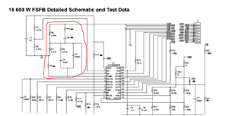
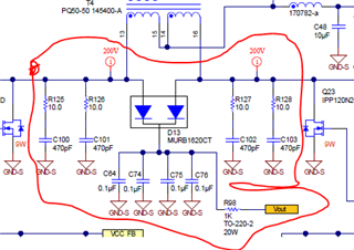
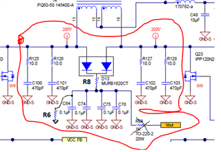
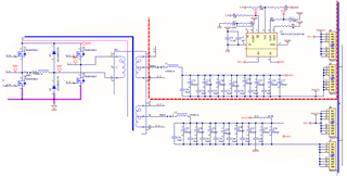
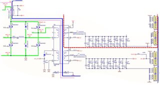
Taking inspiration and learning from 600W evaluation board.

Below are my design specs:

Model 1: 

Input voltage - 200VDC ~ 600VDC

Output - 13VDC ( 84A max, 2A min)

Model 2: 

Input voltage - 600VDC ~ 1000VDC

Output - 13VDC ( 84A max, 2A min)

I will have series of questions related to the design, I will keep posting in the same thread.

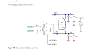
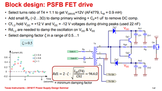
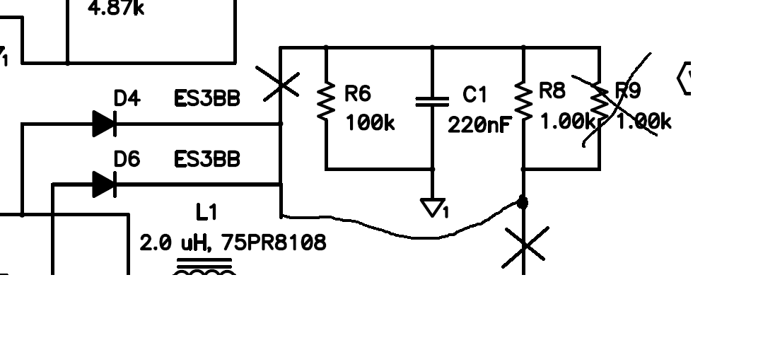
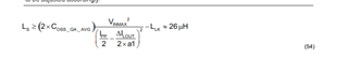
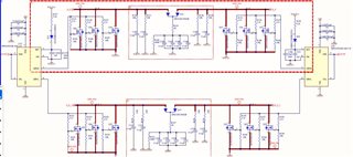
1. Planning to use gate drive transformer for both the models. 

below are calculations for the same. Kindly review and advice

Steps Parameter Value Unit Remarks
1 Peak Voltage (Vpk) 15.00 V Gate driver voltage
2 Min Switching Frequency (Fs) 98000 Hz Datasheet - UCC28950, excel design doc - SLUC222D
3 Time Period 0.0000102 S T=1/f
4 Max Duty cycle ( nominal ) 0.70 % Datasheet - UCC28950, excel design doc - SLUC222D
5 Ton 0.00000714 S  Max duty * Time period
4 Calculated ET 0.00010714 V-S  
  Calculated ET ( micro ) 107.14 V-uS  
5 Calculated ET for bipolar 214.29 V-uS Ton=2*ET/Vpk, for Bipolar drive
6 Source Current Of Gate drive pin 1 A Datasheet(UCC27324P) 
7 Inductance Required 0.0001071 H Ipk=UpkDmax/(Lprim,min*fmin).

2.  At steady state , will duty cycle be 50% or varying ? Since my duty cycle is varying from full load to light load,  Burst Mode or No load, Is there anything to be taken care at the gate drive transformer side. Kindly advice.

3. selected gate driver for now GT04-111-315-B

  • Hello,

    1. Your input range for both designs is 3 to 1 or less.  The excel design tool referenced in application note SLUA560 will be to calculate the required transformer turns ratio, output inductance, output capacitance and all other power stage components.  This information was used to design the 600 W evaluation module.  It sounds like you used these tools in your design.  Please note the transformer turns ratio for both designs will be different and can be calculated with the excel tool based on the input and output power requirement.

    https://www.ti.com/lit/pdf/slua560

    2. If your design is running in CCM per your duty cycle will change with input voltage and not load.  This is how application note SLUA560 recommends that you do the design.

    3. When it comes to the gate drive transformer check the transformer to make sure it can handle the peak, rms current and can operate at your desired switching frequency.

        I reviewed the data sheet for the gate drive transformer and it is rated for 300 kHz and is high pot tested up to 4.5 kV.  It looks like it should work.  However, double check with          the manufacture to make sure it can handle the peak and RMS current you will be driving through it.

    The rest of your specifications look reasonable and accomplishable.

    Regards,

  • Thanks for the response. Yes, the transformer is different based on input voltage range for different models. FYI, Following the excel design document SLUC222D for all calculations. The input voltage range is both fixed ( PFC pre-stage ) and variable ( battery ), But at lower voltage lets say 600, considering model 2,  I will not be operating it in full load, it will be very minimal current consumption but maintaining voltage regulation.

    Commenting on 2nd point on duty cycle, My load conditions are sometimes 85A, 50A, 15A or minimum it can go down to 2A / 4A or sometimes No Load, in all scenarios maintaining voltage regulation. Basically its a varying load.  My understanding is the controller will operate in CCM mode at higher load currents, then maybe less than 15% of load, It will enter DCM mode( setting Rs, Vrs value ), Then further reducing current down to 2A, Controller will have to enter burst mode. Is my understanding correct ? 

    Will the duty cycle have an impact in different load scenarios especially during Transient response, or burst mode of operation? When Ton pulse width reduces during burst mode, My duty ratio will not be 50%,  will it have impact on transferring signal from gate drive transformer ? Please advise

  • Hello,

    Your inquiry is under review and I will get back to you shortly.

    Regards,

  • Hello,

    I thought about this and if you designed a peak current mode PSFB the only way this should go into burst mode is if (duty cycle)*1/fsw < the minimum on minimum on time programed by Rtmin.

    As long as the converter is in CCM with a fixed input voltage the duty cycle will remain unchanged with load.  When the load decreases to a point where the inductor current goes discontinues the duty cycle will change to control the peak and average inductor current to maintain the load and output voltage. 

    If you have the 600 W evaluation module you can evaluate this in the lab.

    Regards, 

  • Ok, I'm still trying to process the information.

    1. I happen to come across this document (Design review of a 2-kW parallelable power supply module (ti.com)), attached image shows gate drive circuit design. Comments on circuit.

    2.  Also If I'm driving silicon carbide FETs using Pulse transformer, I have to restrict VGS to +15V, -5V, is it possible to restrict SIC FETs using this Pulse transformer method ? if Yes, How ?

    3. Read these documents 

    Design review of a 2-kW parallelable power supply module (ti.com) ( Pg 22 ),

    https://www.infineon.com/dgdl/Infineon-GateDriverIC_EiceDRIVER_isolated_gate_driving_solutions-ApplicationNotes-v01_01-EN.pdf?fileId=5546d462700c0ae60170a0c4af851028 ( Pg 6 - 7 ),

    Not able to draw conclusions. why because All most all the Eval boards I have seen both from TI and Infineon , They use Pulse transformer even if the wattage is upto 3 KW. Kindly advice on the robust solution so that i come out of the gate driver design loop and focus on the other design aspects.  Kindly advice whether to go ahead with Pulse transformer ( which most people call it yesterdays solution ) or should go with Isolated gate drive. Give me an argument i can't refuse with reasonable assessment Innocent

    FYI, Eval boards

    1. UCC28950 600W Phase Shifted Full Bridge Design Review/Application Report (Rev. D)

    2. General description Evaluation board EVAL_2kw_ZVS_FB_CFD7 (infineon.com)

  • Hello,

    This is under review and will not be able to be addressed until next Monday due to the US holiday.

    Regards,

  • Hello,

    1. The high side drive looks like they are using a PNP/NPN totem pole driver on the high side FET.  I have seen this used before and it should work.  You should be able to drive these FETs directly with a gate drive transformer as well.

    The benefit of the discreate totem pole driver is it is a discreate driver and will not load the gate drive transformer as much as directly driving the high side FET.

    2.  When it comes to driving SiC FETs in an H Bridge you might be better off using isolated gate drivers.  The UCC21551 is an isolated high side low side driver for SiC FETs.  The following link will bring you to the data sheet for this device.  If you have questions in regards to using the UCC21551 please repost in the e2e with UCC21551 in the thread title.

    https://www.ti.com/lit/ds/symlink/ucc21551.pdf

    3.  I have seen both gate drive transformers and high side/low side drivers used in phase shifted full bridge converters.   The following link will bring you to a phase shifted full bridge design that uses isolated gate drivers vs a gate drive transformer.

    https://www.ti.com/lit/ug/sluub02a/sluub02a.pdf

    It uses to be in high voltage applications you would require to use a gate drive transformer to drive the high side FETs in a half bridge or full bridge.  This is because the FET drivers could not handle the voltage.  However, today with improvements in process and the development of isolated gate drivers, Integrated FET drivers can be used instead of gate driver transformers.

    The benefit of using gate drivers is less circuitry required to driving the high side FETs.  With gate drive transformers you will require a DC blocking capacitor, DC restore capacitor; as well as, protection circuitry to ensure the FETs gates maximum +/- voltages are not exceeded.


    Regards, 

  • Moving on to the other Question:

    On the Secondary side of Transformer winding, i'm Planning to have 2 secondary windings. (shown in fig)

    Reason being, I have to make two models. 12V Variant and 24V Variant.

    The 2 Secondary Windings Will be of 12V and feedback will be taken from One winding.

    For the 12V version two separate windings will be connected in parallel from outside connector.

    For the 24V version, Two secondary windings in Series from the Outside Connector.

    The top secondary winding Will have separate ground. For that I will have a separate isolated power supply and Gate driver. OUTE and OUTF Will be connected to Positive and negative side of Transformer Top side secondary winding. Similarly, to the Bottom secondary winding.

    Your thoughts on this..

  • Hello,

    Your inquiry is under review and I will get back to you shortly.

    Regards,

  • Hello,

    If your are designing a traditional PSFB you will either do a current doubler or a voltage doubler.  These designs would require a center tap transformer on the secondary.  

    I think you are thinking of what you would do with a traditional forwarded converter.  I believe you can still do the same thing with a multi tapped transformer.

    The other option is to use a full wave rectifier on the output instead of SRs.

    Regards,

  • I'm working on the design, I will share once I finish.

    The other question is on Loop compensation.

    I did read the document ( https://www.ti.com/seclit/ml/slup348/slup348.pdf?ts=1702982818805&ref_url=https%253A%252F%252Fwww.ti.com%252Fproduct%252FUCC28951 )

    and thread ( https://e2e.ti.com/support/power-management-group/power-management/f/power-management-forum/1008296/ucc28951-q1-tuning-of-error-amplifier-of-voltage-and-current-control-loop

    My Load current requirements are : No load,  Minimum Load : 2A, Maximum Load : 90A

    But there are different loads ( DC coils, DC heaters, etc )  connected at output drawing different load currents at different instances. 

    In that scenario, will the normal Type - I compensation work or we need a different strategy here. Please advice.

  • Hello,

    I am reviewing your inquiry and will get back to you shortly.

    Regards,

  • Hello,

    I think type 2 compensation should work for your design.  That is what your slide shows.  This compensation has two poles and zero.

    Generally type 3 compensation is generally used in voltage mode control.  This is to deal with double pole in the transfer function that is seen by the output filter pole.

    You had mentioned that your loads are coils.  I am not sure if there is an effect on the control to output transfer function.  You might consider putting place holders for type 3 compensation just in case you need it.

    It is always a good idea to check your compensation with a network analyzer and adjust the loop as necessary.  Some designers prefer to setup the voltage amplifier feedback into an integrator and measure the control to output transfer function and then compensate the voltage loop.   

    Regards

  • When you say Type II compensation or Type III compensation, I will do something similar to what is done in the 600 W App note, with component values taken from my excel sheet. correct??

  • Hello,

    Your inquiry is under review and I will get back to you shortly.

    Regards,

  • Hello,

    What you have circled is type II compensation.  If you populate R28 and C8 you you will have type III compensation.

    Please note that the excel spread sheet is setup for type II compensation.

    Regards,

  • Hello,

    The following link will bring you to a paper that discusses the difference between Type II and Type III amplifier compensation feedback.

    I believe you will find this paper helpful in your design efforts.

    https://www.ti.com/lit/an/slva662/slva662.pdf

    Regards,

  • Ok. Moving on, Suggest me design for Snubber circuit on the Synchronous rectifier MOSFETs.

  • Hello,

    Your inquiry is under review and I will get back to you shortly.

    Regards,

  • Hello,

    The following information was for setting up snubbers across SRs in flyback converters.  However the technique and math for setting up the snubbers in SRs is similar for a PSFB.  You should be able to use this information to setup the snubber on your SRs in your design.

    Regards,

  • I was going through EVM (600 w) and (PMP8740 2kW) designs, both have used RCD snubber. 

    can you guide something related to this type of design, like calculating components values, etc. 

    Also, what do you suggest? 

  • Hello,

    Your inquiry is under review and I will get back to you shortly.

    Regards.,

  • Hello,

    D13, C64, C74, C75, C76 and R98 form an RCD clamp.   I do think there is a better way to setup an RCD clamp for this application.

    The following link will bring you to an e2e thread discussing how to setup and RCD clamp for this application.

    https://e2e.ti.com/support/power-management-group/power-management/f/power-management-forum/1132532/ucc28950-ucc28950-senkron-rectf-snubber-question/4202839?tisearch=e2e-sitesearch&keymatch=UCC28950%2520Clamp#4202839

    Regards,

  • Ok. There is some confusion based on what you're suggesting in the link. R8 another end will be left unconnected, R6 and C1 other end where it should be connected??

    1.Can you please draw and share.

    2. Where should Vout be connected?

    3. Some formulas are valid, and some have changes. Can you mention the list of formulas which are correct and can be utilized?

    4. Should Both diodes be selected based On Iout ?

  • Hello,

    Your inquiry is under review and I will get back to you shortly.

    Regards,

  • .Hello,

    Answers to 1 and 2.

    In the post they are using and RCD clamp.  It is not connected to the output.

    I have marked up your schematic to show where R6 and R8 would be placed.  R98 would be removed.

    3. Which formulas in the post are not valid?   Are they clarified and correct in the post?

    4.  The current that goes through the diodes is the current that is present in the leakage inductance when the FET turns off.  The actual current in the SR when the FET turns off is (Iout - (Change in ILout/2.)  Using Iout is an over estimate but O.K.  Over estimating is O.K. when setting up the clamp.  Under estimates is where you will run into issue.

    Regards,

  • On the diode part, from excel sheet 

    Iout (I Lout_RMS) is 89.82.

    Δ lLout is 17.85.

    = 89.82- (17.85 / 2 ) = 80.895 A to be considered during selection. Is this correct??

    2234.SLUC222D.xls

  • Hello,

    You are inquiry is under review.  I will get back to you shortly.

    Regards,

  • Hello,

    Mathematically you are correct.  However, you probably want to multiply by a factor of 1.2 to 1.3 for margin.

    Regards,

  • Ok. Got it. Can you please explain in brief the operation of the clamp circuit. Especially 1K resistor not being connected to output and being connected between diode and caps. I was of understanding that thru Vout capacitor would be charged , something like that. But Please share your deep insights.

  • Hello,

    Your inquiry is under review.  I will get back to you shortly.

    Regards,

  • Hello,

    The purpose of an RCD clamp is to protect the FET from an over voltage caused by the leakage inductance energy and ringing that may be present on the switch node.  So when the FET turns in this application 2XVout will be stored across C74..C76, and C64.  Resistor R8 is used to dissipate the magnetizing energy and protect the FET from an over voltage when the SR FET turns off.

    The power dissipation in R8 in the traditional clamp would be cause by the secondary leakage inductance.

    Pslk= ((Llsk/2)*(Iout)^2)*fsw


    If you use the clamp with R98 tied to the output the power dissipation of the resistor would be ((2*Vout)-Vout)^2)/R98.  This clamp will work well but most customers find that it dissipates too much power.

    Regards,

  • Ok.

    1. Regarding The equation of PSlk, since the output inductor frequency ( 2 • fsw ) will be twice that of operating frequency , in my case ( fsw: 100kHz ) , so the equation should be fsw or 2•fsw ??

    2. During operation this process of charge and discharge would be continuous, and the only way to discharge each cycle is thru R6. Is 100k a good value to begin with ?

  • Hello,

    I am reviewing your inquiry and will get back to you shortly.

    Regards,

  • Hello,

    Please see my comments below.

    1. Regarding The equation of PSlk, since the output inductor frequency ( 2 • fsw ) will be twice that of operating frequency , in my case ( fsw: 100kHz ) , so the equation should be fsw or 2•fsw ??

    > Even thought the inductor is seeing 2*fsw the switch is not.  It is switching at fsw.

    2. During operation this process of charge and discharge would be continuous, and the only way to discharge each cycle is thru R6. Is 100k a good value to begin with ?

    > R6 is meant to discharge the capacitor every switching cycle to ensure that capacitor does not creep up above 2*Vout.  A 100 k should be fine.

    Regards,

  • going to back Two windings option:

    1. The question is, My total secondary output current is 89.82A. Since i have two windings, my current will be divided. As per the excel sheet, output inductance is 2.55uH. since My current will be halved, my inductance value should be twice that of calculated value as per below formulae, i.e.  5uH. is that correct ?

    2. Also, while selecting inductor, how many times should be Isat value?

    3. What is the core material to be used for magnetics, Shim inductor, Output inductor? is there any specific? Below are the specs which i got from one of the eval boards?

    4. The output voltage is regulated to 13V. Let's say i want to have overvoltage protection, what is the design approach?   Considering 1 V allowable Output voltage transient, meaning transient Overshoot should not be detected as Overvoltage.   Also Let's consider it takes 1Second to settle back to 13V.

    share any reference circuit design.

    5. I have sent a friend request, please do accept it. I will share schematic for review.

  • Hello,

    I am reviewing your inquiry and will get back to you shortly.

    Regards,

  • Hello,

    Please see my comments below.

    1. The question is, My total secondary output current is 89.82A. Since i have two windings, my current will be divided. As per the excel sheet, output inductance is 2.55uH. since My current will be halved, my inductance value should be twice that of calculated value as per below formulae, i.e.  5uH. is that correct ?

    >In the excel tool the inductor selection is based on a single inductor, also in the question there is a multiple of 2*fsw (Primary frequency).

    >So if you are selecting one of these Ls then you would remove the 2 in the above equation.  Cange ILOUT would be divide by 2.  The inductance will come out to be the same value.

    2. Also, while selecting inductor, how many times should be Isat value?

    > Generally 1.5 to 2 is good.

    > The inductance at max load needs to be close to what is calculated.

    3. What is the core material to be used for magnetics, Shim inductor, Output inductor? is there any specific? Below are the specs which i got from one of the eval boards?

    >Generally for my inductor designs I give the peak and RMS current requirements; as well as, voltage requirements to a magnetic manufacturer like Wurth or Renco to do a custom design.

    >If you are doing your own design Mag-Inc has application note that can help you with this process.


    4. The output voltage is regulated to 13V. Let's say i want to have overvoltage protection, what is the design approach?   Considering 1 V allowable Output voltage transient, meaning transient Overshoot should not be detected as Overvoltage.   Also Let's consider it takes 1Second to settle back to 13V.

    share any reference circuit design.

    > The UCC38951 does not have over voltage protection you would have to design it discreetly.

    > You could use a hysteretic comparator and pull SS to ground to shut down the FETs on the case of an over voltage.  Once the fault is cleared the design will be soft started.

    5. I have sent a friend request, please do accept it. I will share schematic for review.

    >All of my e2e support is through the forum.  If you need your schematic reviewed can share it on this platform.  You should be able to post it into the thread.

    Regards,

  • 1.  both windings work together as separate outputs. Meaning there will be two 13V supplies running parallel to each other.  My understanding is that, in that case both the inductors will see 2 * fsw at any instant, as they work in parallel to each other. Cange ILOUT would be divide by 2. Which leads to cancellation of both the 2's in the equation and, hence doubling the inductance. Please advise.

    5. Working for a customer, not to land in trouble at later point of time. Thats the only concern.

  • Hello,

    Your inquiry is under review and I will get back to you shortly.

    Regards,

  • Hello,

    Can you show me a schematic of the transformer and output circuitry for this design?

    Regards,

  • Hello,

    After reviewing your schematic and seeing that you have two center tapped secondary windings, you are correct in regards to selecting your output inductors for this design.

    Regards,

  • Ok. Thanks for the Inputs.

    Moving on, 

    1. For the shim inductor selection, the value is 13.62uH from excel. Should i keep the same value as per above two center tapped secondary windings design?

    2. Also to maintain ZVS across the entire load range, Should the inductance be as per excel or needs to be increased or decreased?


    3. What are the Output voltage levels of OUTE, OUTF signals? 

    4. Suggest a gate driver design (focusing on SiC MOSFETS) for Primary side Fets.  And also, Their Bias supply generation designs if available. Lesser design time approach will be best.

    5. Planned to drive above two Centre-Tapped secondary windings in the below manner.

    FYI,

    Vout1+, Vout1- : top winding

    Vout2+, Vout2- : Bottom winding

    Vout1+ is the supply which is generated during startup phase with no load conditions, i.e. When OUTE, OUTF are disabled. Vout1+ will be the bootstrap supply. Please let me know if any changes.

  • Hello,

    Your inquiry is under review and we will get back to you shortly.

    Regards

  • Hello,

    Please see my comments below.

    1. For the shim inductor selection, the value is 13.62uH from excel. Should i keep the same value as per above two center tapped secondary windings design?

    >The excel sheet will calculate the Ls to achieve ZVS down to 50% load. 

    2. Also to maintain ZVS across the entire load range, Should the inductance be as per excel or needs to be increased or decreased?


    >If you want to achieve ZVS down to a lower power level change Ipp/2 in equation 54  based on where you want to achieve ZVS.

    >If you want the design to achieve ZVS to 25% load change Ipp/2 to Ipp/4 in equation 54.

    3. What are the Output voltage levels of OUTE, OUTF signals?

    >These levels can be found in the data sheet. https://www.ti.com/lit/gpn/ucc28951


    4. Suggest a gate driver design (focusing on SiC MOSFETS) for Primary side Fets.  And also, Their Bias supply generation designs if available. Lesser design time approach will be best.

    >The following link will bring you to an application note that shows how to design a phase shifted full bridge.  It does use standard FETs.

    https://www.ti.com/lit/pdf/slua560

    > I would suggest using SiC FET drivers.  The following link will bring you to the select that TI has for FET half bridge drivers.

    https://www.ti.com/power-management/gate-drivers/half-bridge-drivers/overview.html

    >If you have questions on how to use these FET drivers driving SiC FETs.  Please repost so the appropriate applications engineer can answer your question.

    Regards,

  • Thanks for the inputs.

    1. Please evaluate the design mentioned in the 5th point.

    2. When you say for low power it's Ipp/2, it's already Ipp/2 in the equation. Further I should do ( Ipp/2 )/2.  Please clarify. 

    3. I want to achieve ZVS down to burst mode or light load conditions, what will be equation or value to be considered?

    4. For the shim inductor selection, the value is 13.62uH from excel. Should i keep the same value as per above design which I have implemented or it needs to be doubled or halved . As you can see the design with two center tapped secondary windings design?

  • Hello,

    1. Please evaluate the design mentioned in the 5th point.

    > Your schematics look to be functionally correct.

    > You can use the excel design in the product folder to check the power stage and controller setup.

    2. When you say for low power it's Ipp/2, it's already Ipp/2 in the equation. Further I should do ( Ipp/2 )/2.  Please clarify. 

    > 1/2 = 50%,  1/4 = 25%, 1/10 = 10%

    3. I want to achieve ZVS down to burst mode or light load conditions, what will be equation or value to be considered?

    >You just need to change Ipp/2 based on the minimum load you want in equation 54.  If you want it to go down to 10%load this would be Ipp/10.

    4. For the shim inductor selection, the value is 13.62uH from excel. Should i keep the same value as per above design which I have implemented or it needs to be doubled or halved . As you can see the design with two center tapped secondary windings design?

    >You are running to parallel windings on the output.  Depending on the loading of each phase will affect the ZVS on the primary.

    Regards,

  • Ok.Thanks for the inputs.

    I have started using the EVM. There is input supply of 400VDC,

    Then I followed the same procedure as mentioned to turn on the EVM, but the output voltage is 0. NO LOAD condition. 

    Also I was able to see signals on A,B,C. NO pulses from OUTD. Please assist. 

  • Hello,

    Those EVMS are tested 100% before they leave the factory.  So I am not sure why yours has an issue.  If out A, B and C are switching and D is not is not that is strange.  Could you double check this and look at the outputs directly at the output output of the UCC28951 to confirm?

    Regards,