This thread has been locked.

If you have a related question, please click the "Ask a related question" button in the top right corner. The newly created question will be automatically linked to this question.

UCC28711: UCC28711:

Part Number: UCC28711
Other Parts Discussed in Thread: UC3844, UCC28C44

1. In the case of UCC28711, the DRV pin is indicated as a current source. Additionally, the maximum voltage is limited to 14V (generated by the diode)

2. In contrast, for other ICs, voltage is applied (see diagram below).

3. For the UCC28711, if the output of the drive pin is set as a current source (maximum 0.035A), how is the VGS voltage applied to the Mosfet adjusted? Is the maximum VGS determined by the Qg characteristic of the Mosfet?

4. The gate resistor is a component that adjusts the turn-on/off time. When supplied as a current source, how is this adjusted?
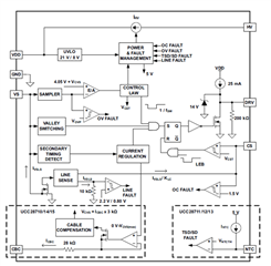
<UCC28711>
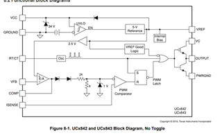
<UC3844>

  • Q: If the voltage on the VS pin is due to voltage division by the auxiliary winding, it is assumed that the ringing voltage waveform will be fed into the input. The standard voltage value of 4.05 V for the VS pin in the datasheet would be a DC value. Is it filtered by the internal sampler to produce a DC value? Can you provide a rough idea of how AC values are sampled to DC values?

  • Hi Seungpyo,

    Thank you for reaching out.

    The Vs pin sees a scaled replica of AUX winding waveform. So the initial ringing is basically neglected (leakage) so get a good sample for o/p voltage. There are certain timing constraints to be met to get a good sample. This is detailed in the datasheet pages 13 and 14. We cannot share the details of internal sampling, but all it needs is the external circuit (mainly the leakage inductance and parasitic capacitance) affecting the waveform to be controlled so that the timing constraints of the Vs pin is adhered to. Else there will be fault encountered.

    The current 25mA will charge the gate capacitor (i = cdv/dt). As soon as the voltage reaches 14V it will be clamped to this value. The gate resistor only slows/ quickens the rise or fall time and hence the transition times.

    Regards,

    Harish

  • I'm ultimately curious about what output voltage is applied to the DRV pin.

    The DRV pin is connected to a diode that allows a maximum Vgs of 14V. And there are VDD(Maximum 38V), current source of 25mA.

    So, is the value of sum voltage of VDD and the current source of 25mA applied to the MOSFET Vgs connected to DRV?

    If not, is only the 25mA applied to create the MOSFET Vgs, as mentioned in the previous response? (If only 25mA is applied, please explain the role of VDD.)

    Also, I'm curious about the role of the 200k resistor.

    Lastly, if the output of DRV is indeed 25mA, I assume that the Vgs would vary depending on the type of MOSFET. Would it be correct to think that the gate resistance connected to DRV in the case of a current source only operates during turn-off?

    I used to use the ucc28c44 before, and that model had VDD directly connected to the OUT pin, so the output voltage was clearly predictable, but this model confuses me.

  • Hi Seungpyo,

    Thank you for reaching out.

    The DRV pin is always clamped to 14V by the diode. 25mA will be the source current coming out of this pin.

    200k connected across the gate so that the MOSFET gate is discharged.

    The gate resistance will have an effect on both turn on and turn off.

    Regards,

    Harish

  • I understood your metion.

    I wonder purpose of Vdd conncted with 25mA.

  • Hi Seungpyo,

    It is used for internal bias voltage, I am not sure how it is implemented internally (may be something like voltage controlled current source).

    Regards,

    Harish