This thread has been locked.

If you have a related question, please click the "Ask a related question" button in the top right corner. The newly created question will be automatically linked to this question.

UCC28180EVM-573: Power management forum

Part Number: UCC28180EVM-573
Other Parts Discussed in Thread: PMP31164, UCC28180, , UCC256404, UCC2818, UC3854

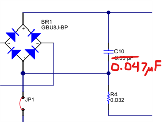
We have modified the UCC28180EVM similar to PMP31164 reference design except below changes:

1. Boost inductance 0.9mH 

2. Frequency 140kHz 

3. Current sense resistor 0.1ohms for 100W.

4. Icomp 1000pF, Rseriescomp= 130Kohm, Cseriescomp, = 470pF(Type II compensation)

5. Rvcomp =47Kohm, Cvcomp=4.7uF and Cvcomp,parallel = 47nF.

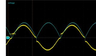
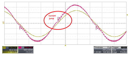
Previously we have tested we observed more distortion in the waveform

After adding type II current compensation the THD got little better. But still i seeing ac input current is not starting from zero 

I dont know why the current waveform is not starting from zero. How do i avoid this? Please help me

  • Hello Ramahadullah, 

    Can you please provide the ICOMP waveform (1V/div) that corresponds to this input current.
    Also, whenever you show a waveform, please include the test conditions under which the waveform was obtained. 

    I wonder if ICOMP voltage is held lower than it should be at the zero-crossings.  This would allow a wider than normal duty-cycle and that may account for the extra current at the crossings. 

    Regards,
    Ulrich  

  • Hi Ulrich 

    Attached the waveform with ICOMP. The testing is performed at 50W load.

    Also attached the zoomed waveform of Vds and Input Current. 

    Is it anything related to current amplifier saturation ?

    How can i avoid this? Please help

  • The second image input current probe is not degaussed while capturing the waveform. Please scale the magnitude to 1/100 times. Sorry for the inconvenience.

  • Hello Rahamadullah, 

    Thank you for providing these waveforms.  
    There is no indication of CA saturation in the ICOMP waveform.  Actually, it doesn't tell me as much as I thought it would. 

    On the other hand, your second waveform of Vds is very helpful.  You can see where the current becomes distorted around the zero-crossing, the Vds peaks for each switching cycle no longer reach the output voltage level.  This tells me that the drain current (peak inductor current) is not high enough to full charge up the total switched node capacitance at the drain.  And that tells me that the MOSFET is too big for the application. 

    You mentioned that you modified the UCC28180 EVM with different inductor, some compensation components, Rsense, and higher frequency. 
    I assume then that the 360W EVM still has the original SPP20N60C3 MOSFET and C3D04060A SiC diode.  These parts have much higher parasitic capacitances than necessary for a ~100W application. 

    I suggest to replace the EVM semiconductors with STP10N60M2 and C3D02060A (or similar) which have much smaller Coss and Cj.  
    They also are rated for lower current, but your application is lower current so conduction losses will still be low. 

    I think these switch sizes will help clean up the input current waveshape.  

    Regards,
    Ulrich

  • Hi Ulrich

    That was a good catch. We have ordered new mosfet to test it. Meanwhile we have reduced the frequency from 140khz to 65kHz the waveform at zero crossing got little better. 

    Thanks for your input. It really helped a lot.

    Regards

    Rahamadullah

  • Hi Ulrich

    We have tested the PFC with a different mosfet that has Coss of 20pF (3.5 times lesser than the mosfet used in UCC28180EVM-573). I have seen little improvement on the falling half wave of 400Hz input current waveform without any distortion at zero crossing. But still the problem did not vanish. I could see the similar behaviour at rising half wave of 400Hz input current.

    I have seen similar problems that has been discussed in the TI forum (https://e2e.ti.com/support/power-management-group/power-management/f/power-management-forum/1179479/ucc28180-ucc28180-pfc-and-thd-issue)

    But i dont know what is the final solution that had been suggested for that query.

    Note: I have connected UCC256404EVM as a load to the PFC.

    Will the HV pin on the UCC256404 connected to the AC supply is causing this input ac current waveform distortion at zero crossing (only at each rising half wave of 400Hz input current and on the falling half wave of 400Hz input current waveform is proper without any distortion) ?

    I am sharing my mail id here (rahamadullah.abdullatheef@boeing.com). 

    Thanks in Advance

    Regards

    Rahamadullah

  • Rahamadullah,

    Please give us few days to respond.

    Thanks,

    Ning

  • Yes Ning. Thanks for your reply.

    Uploading few waveform for your reference that may give you better insight about the problem.

  • Hello Rahamadullah,

    Thank you for your patience while I try to understand what could be happening to cause the jump in current in this situation.  
    The waveforms are very helpful. 

    First of all, in the last waveform (immediately above) with input current and rectified input voltage, it can be seen that the current appears to jump exactly at the 0V point of the voltage.  I am certain that this is not possible, and I believe that the jump is actually occurring about 80~100us to the right of the zero-crossing. 90-degree displacement current in X-capacitors in the EMI filter is shifting the total AC current to the left (leading phase-shift).  

    But that does not account for the current jump.  Often there can be residual voltage stored on a capacitor after the diode bridge which accounts for a jump, but it is evident that there is no such voltage.  Another possibility is that the ICOMP amplifier becomes saturated low and allows excess duty cycle as the input voltage rises until the amp can come out of saturation.  But looking at the ICOMP waveform above, it does not appear to be saturated (although I am not sure of this).

    One other possibility that occurred to me is that perhaps the bridge diodes have long reverse recovery time which does not affect 50Hz operation significantly, but may have this consequence at 800Hz input.  
    Following up on this possibility, I request that you try replacing the existing diode bridge with a bridge or separate diodes that have fast recovery time.  I don't think they need to be ultrafast, but definitely much faster than standard-recovery diodes. 
    Please try this idea.  I hope it reduces or eliminates the current jump. 

    Besides that, I also ask to try adding a pull-up resistor from VCC to ICOMP to add a small bias current to ICOMP.  The purpose is to try to pull the ICOMP voltage during the zero-crossing up a little higher, or make the ICOMP amp work to keep the voltage low.  If there is any saturation, this may help reduce that.  Please try this idea independently of the fast-recovery diodes.  
    For lack of any better idea, I suggest a pull-up current of about 11uA when Vicomp is ~1V.  If VCC is 12V, then (12V-1V)/11uA = 1Megohm.
    If that shows improvement, then try increasing the current (lower resistance) gradually until performance begins to suffer.
    It's possible that bias current < 11uA may perform better, so that can be investigated, too.

    If that doesn't help, another alternative to try is to add a load from ICOMP to GND instead of a pull-up. 
    Try varying the load up or down around a 10uA starting point when Vicomp = 1V. 

    Please let me know if any of these ideas bear fruit to improve the current waveshape at the zero-crossing.   

    Regards,
    Ulrich

  • Hi Ulrich

    Thanks for the reply. 

    1. I tried with 50Hz input frequency as well. The current jump is still observed at zero crossing. So we confirmed that it is not a rectifier diode current recovery issue.

    2. Tried adding pullup on ICOMP pin through VCC from 1Mohm to 150Kohm. At 500Kohm the THD was better improved from 9.8% to 8.1%. But still the current jump was observed. From 1Mohm to 500Kohm the THD was reducing and from 500Kohm to 150Kohm there were no change observed.

    3. Tried adding pull down resistor ranging from 150Kohm to 1Mohm. No significant changes observed.

    Note: If 400Hz is the problem why the current jump happening at 50Hz as well?

    Is there anything that i am missing here in the circuit? Please advise

    Regards

    Rahamadullah

  • Hello Rahamadullah,

    At the beginning of this thread, you said you modified the UCC28180 EVM to be similar to PMP31164.
    The EVM normally has 0.33uF at C10, just after the diode bridge BR1.
    PMP31164 has a 0.1uF cap at that location, but also has a 100uH Diff-Mode choke in series. 
    Did you change the EVM to include these parts? 

    In any case, I request that you reduce whatever cap is there to 0.047uF and see if the input current step improves.

    The value of 0.047uF is not calculated, but merely a quick guess at a lower value to test for the effect of stored charge when Vin is at the zero-crossings. 

    Your waveform above shows clean valleys at the zero-crossings, but I don't know where this voltage was measured.

    Previously, I didn't advise to reduce this cap value, because the waveform suggested that there was no evidence of residual voltage, but if that voltage was measured elsewhere other than across C10, then the possibility of residual voltage causing the current step is still valid. 

    Please try reducing the cap value as shown, and see what happens to the input current.

    Regards,
    Ulrich  


  • Hi Ulrich

    The rectified voltage is measured exactly at C10 (in our case as per PMP31164 C10 is after the DM choke). 

    I have changed the C10 value from 100nF (film cap) to 47nF (film cap) value previously but found no significant changes.

    Note: I have removed all X caps which was there between the input line ac voltage connector and before the diode bridge to avoid extra reactive current.

    Regards

    Rahamadullah

  • Hello Rahamadullah, 

    From your previous post:

    Note: If 400Hz is the problem why the current jump happening at 50Hz as well?

    Is there anything that i am missing here in the circuit? Please advise

    Apparently there is something that we are both missing, because I have given you everything that I can think of and I don't have any more ideas. 

    At this point, all I can do is suggest the procedure that I would use to debug this problem.   I suggest to: 
    1.  Concentrate on the interval +/- 200us (or less) around the voltage zero-crossing.  Ignore the rest of the line cycle.
    2.  Have a current probe on AC input, a probe on inductor current, and a probe on MOSFET drain current.  If you don't have that many probes, you'll have to move one of them around. 
    3.  Voltage probe on rectified Vin (across C10), on UCC28180 DRV pin, on MOSFET gate pin, and on MOSFET Vds.
    4.  Compare inductor current to AC input to ensure that all of AC input goes into inductor.  The inductor should have exactly the same current step as the AC. This rules out any side paths.  
    5.  Compare MOSFET drain current to inductor current.  Line up Ids with DRV signal and Vgs signal and Vds signal.  
    6.  Look for situations where DRV signal shuts off but Vgs is delayed off, and/or Vds stays low too long which may allow inductor current to rise too fast. 
    7.  Compare voltage across inductor with di/dt of current to verify that V/L = di/dt applies correctly.  No other cause of current step.
    8.  Put V-probe on ICOMP and examine these waveforms with and without 500kR pull-up on ICOMP.  See how changes in Vicomp affects DRV duty cycle and drain current.
    9.  Keep in mind that the UCC28180 generates PWM duty cycle by comparing the ICOMP voltage to an internal ramp and uses Leading-Edge Modulation.  This means that each switching cycle starts with DRV off, and DRV turns on when the ramp rises above Vicomp.  Higher Vicomp means longer off time and lower duty cycle.  There is an internal offset of about 0.72V above GND (I'm not sure of the exact value) for both ramp and Vicomp. 
    10. From results of all of the above, think of what would have to change (or change more) to make the inductor current rise more slowly and what would be necessary to make that change happen. 

    Regards,
    Ulrich

  • Hi Ulrich 

    I really appreciate your effort replying to our queries.

    We tried implementing your suggestions but the results were not satisfying except that improvement i mentioned in previous mail.

    We tried evaluating UCC28180 as per PMP31164 reference design for avionics the results are not satisfying for 400Hz and 800Hz input. There is a current jump issue we are seeing in the input current at every zero crossing and we see similar behavior in the PMP31164 test results as well. Because of this the THD and harmonics magnitudes are beyond our requirement limits. We are suspecting this issue is due to absence of feedforward input voltage sensing as per few research papers.

    1. https://ieeexplore.ieee.org/stamp/stamp.jsp?tp=&arnumber=7869710&tag=1

    2. https://ieeexplore.ieee.org/stamp/stamp.jsp?tp=&arnumber=4517000&tag=1

    We are planning to move forward with older ICs like UCC2818 and UC3854 series which has input feed-forward sensing that could help us with the problem we are facing right now.

    Do let me know your thoughts.

    Thanks

    Regards

    Rahamadullah

  • Hello Rahamadullah,

    You may be right; the UCC28180 certain has few pins to work with and much of the functional blocks are inaccessible to attach modifications which might help reshape the current.  The older devices have more pins and access points into which compensating signals may be applied. 

    Given your reply above, I will close this thread. 

    Regards,
    Ulrich