This thread has been locked.

If you have a related question, please click the "Ask a related question" button in the top right corner. The newly created question will be automatically linked to this question.

TPSI3050: Design with TPSI3050

Part Number: TPSI3050

Hello team,

I am trying to use the TPSI3050S to drive the Power MOSFET to control the power supply lines. the expectation for our application is 100% ON.

From the datasheet  maximum duty cycle we can obtain is 93% i would like to know during the remaining 7% time what is logic state of EN pin and VDRV pin.

  • Hello prema,

    Thanks for reaching out to our team on E2E! Don't use the S-variant of the TPSI3050, use the regular TPSI3050. You can ignore the power transfer duty cycle when considering driver switching timing. If your EN is 100% ON, VDRV will be 100% ON. 

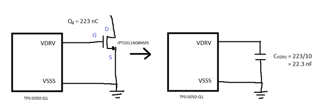
    We can model switching a MOSFET as charging and discharging a capacitor (CVDRV), the value is determined by the total gate charge (Qg) divided by the driver voltage (VDRV). Every time we turn on the MOSFET, this is the same as charging up CVDRV to 10 V. Every time we turn off the MOSFET, we discharge CVDRV

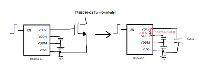
    When the TPSI305x-Q1 drives VDRV high, it basically connects VDDH to VDRV. When the TPSI305x-Q1 drives VDRV low, it pulls VDRV to VSSS. The  peak source and sink currents (1.5A/3.0A) can approximate what the internal resistance looks like for pullup/pulldown.

    When you first power the device, the power transfer charges CDIVx. When you turn the driver on, it charges CVDRV via CDIVx. The voltage of CDIVx drops since all the charge must be shared with CVDRV. Then, the power transfer needs to replenish the charge in CDIVx. The voltage drop is shown as droop in the calculator tool. So turning the MOSFET on once for 6 seconds, 6 days, or 6000 days, all requires the same amount of charge. 

    Best regards,
    Tilden Chen


    Solid State Relays | Applications Engineer

  • Hello Tilden,
    Thank you for your reply,

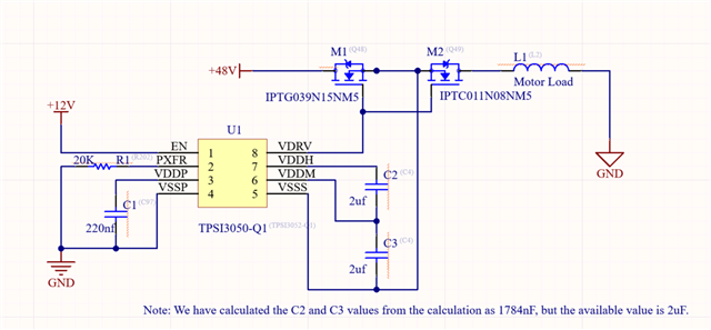
    We are planning to use TPSI305x-Q1 (Driver) and IPTC011N08NM5 (MOSFET) for our design and Also,we are going with two wire mode design and below attached schematic snap.kindly check this selected value on this schematic.

    MOSFET Qg = 446nC

    1.what is the minimum & maximum VDRV pin (Iout current)? how can we calculate the Iout current for our design?

    2.Panasonic recommended GATE resistor for their driver circuit, as shown in the attached snippet. We are planning to use TPSI305x-Q1 (Driver) and IPTC011N08NM5 (MOSFET) for our design. Could you please confirm whether that gate resistor is needed for our design? If it is needed, then how can we calculate the gate resistor for our design?.

  • Hello prema,

    Thanks for your reply. I replied in the other thread so closing this one.

    Best regards,
    Tilden Chen


    Solid State Relays | Applications Engineer