This thread has been locked.

If you have a related question, please click the "Ask a related question" button in the top right corner. The newly created question will be automatically linked to this question.

TPS552882: High inherent power draw, and apparent low efficieny

Part Number: TPS552882
Other Parts Discussed in Thread: CSD15571Q2, CSD16301Q2

Hi,

We're building an LED matrix display, and are using two independant TPS552882 power supplies. The design criteria for these two supplies is as follows:

  • White LED supply: Vin 9-15 V, Vout 5 V, Iout <4.32 A
  • Red LED supply: Vin 9-15 V, Vout 9.6 V, Iout <1.20 A

We've received our first prototype PCBAs, and the design does not work as expected. Notably, the 5 V supply gets too hot to touch, and the board draws 9 W on the input. We have shunt resistors for measuring the outputs from both TPS552882 supplies, so I disconnected these (thereby dropping all load from the supplies) and still measure 8.7 W draw - and the 5 V supply continues to get hot in operation. I don't have a thermal camera to know where the energy is going exactly - but it feels like it's the inductor.

I should note the output voltage on both supplies is correct (5 V and 9.6 V respectively), and I can even put additional load on the supplies. A 20 W load on the output still measured at 4.9 V - however the efficiency was only around 50-60%.

Yesterday, on another PCB, we spent some time trying different things. As we have two supplies, we tried swapping feedback resistors between them - the 9.6 V supply that seemed okay became very hot when set at 5 V. This test was not entirely comprehensive, as we didn't also change the compensation network. We did try swapping the inductors, and that didn't appear to have any effect (though we didn't measure output ripple, just output voltage, nor did we attempt to load the supply).

With no changes to the design, i.e. testing the schematic shown below, we measure 2 Vpp ripple on Vin (supplied with a quality bench power supply). With such a high ripple, I also measured the EN/UVLO which showed a lesser ripple and remained above 4 V.

One thing I noticed, upon reviewing our design against WEBENCH, is that our M2 MOSFET is not on the list of alternatives. We have the CSD15571Q2 in both the M1 and M2 positions for both supplies - however I couldn't find any design notes about the parameters of these FETs. Given our supply isn't operating correctly in low-load conditions, I figure the FET itself likely isn't the problem?

In any case, here's our two supplies:
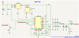
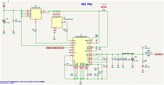
Note the sequencing using the VCC and PG from the white supply to enable the red supply. We did suspect this may cause issues, and removed the white supply entirely (FETs, SMPS IC, etc) to try eliminating this as a cause. We were able to convert the red supply to 5 V (ignoring compensation network changes, and using the 4.7 uH inductor) and demonstrate the fault was still apparent.  I should also note we've spent most of our time testing in the buck configuration. We did show the boost mode is functional, but we didn't do much more testing than that.

We've ordered some replacement FETs, the CSD16301Q2, which the WEBENCH recommended in both M1 and M2 positions. We've also ordered the TPS552882EVM-400K kit for further testing and experimentation.

Can you please review and comment on our design? I've been unable to simulate the design in WEBENCH (seems not available?), and I'm not sure exactly what this fault condition is caused by.

Kind regards,

Dan

  • Hi Dan,

    Thank you for reaching out. The schematics are not clear. So please attach a clear PDF version. Please provide part number or datasheet of each output capacitors.

    Primarily, please try to change white PSU R16 to 10kohm to see if it is stable. Also, can you help provide Vin Vout SW inductor current waveforms?

    Regards,

    Mulin

  • Hi Mulin,

    Thanks for helping us with this. I've attached PDF pages, one for each supply. Let me know if I've missed any details.

    Input and output capacitors for each supply is a mix of 22 uF ceramic caps, and 220 uF electrolytic. Datasheets here: Datasheet - LCSC Electronics and Datasheet - LCSC Electronics.

    I'm not really sure how to get you current waveforms - perhaps you can explain this a bit more? I've got a multi-channel oscilloscope and have attached waveforms for the input, output and the inductor (measured at SW1).

    Swapping R16 from 261 K to 10 K made a huge difference - the power supply is quiet, cool and very stable. I checked against the WEBENCH output, and the component value we'd selected was the recommended value. Can you explain what's gone wrong here?

    White supply input (measured at C35)

    White supply output (measured at C22)

    White supply inductor, measured at U4-D

    schematic_part-White Supply.pdf

    schematic_part-Red Supply.pdf

    Kind regards,

    Dan

  • With that 10k resistor, and ignoring about 400 mW of unrelated power draw on the PCB, I measure 22.8 W in and 19.6 W out - which gives 86% efficiency! I haven't compared this with the expected graphs, but that's certainly more in line with our expectations. The inductor is getting hot, but not hot enough that I can't touch it - and that's a big step up from earlier where the inductor was too hot in the no load condition.

  • Hi Dan,

    I think unsuitable compensation parameters causes problem. WEBENCH parameters are just for reference, so some parameters should be optimize in real applications. In buck mode, the cross frequency is higher than boost mode and phase margin will drop, that's why boost mode is functional. After change R16 to 10kohm, cross frequency drops and phase margin increases.

    About schematic, below is my feedback.

    White LED supply: Vin 9-15 V, Vout 5 V, Iout <4.32 A

    1. Add a 0402 0.1uF ceramic capacitor in VDC net and put it as closely as to chip.
    2. C3 package is too large and will cause problem in layout. Recommend to use 0603 package with higher than 16V voltage range.
    3. Recommend to set R7=44k to set ILIM=7.5A.
    4. With 400kHz fsw, use 4.7uH inductor because of device internal stability requirement. 2.2uH may cause instability. So recommend to choose 4.7uH inductor with Isat>7.5A.
    5. Strongly recommend to add RC snubbers (330pF+2.2ohm(1206 package) ) in SW1 and SW2 pins as EVM. Make sure the snubber in SW2 side is populated.
    6. Add a 0402 0.1uF ceramic capacitor in Vout pin  and put it as closely as to chip.
    7. Will you use output current limit function? If use, ISN and ISP pin should be connected as below.
    8. With 4.7uH inductor, recommended compensation parameters. :R8=1kohm, C6=15nF, C7=22pF.

    Red LED supply: Vin 9-15 V, Vout 9.6 V, Iout <1.20 A

    1. Follow same advice as white.
    2. Recommend to set R16=82.5k to set 4A inductor current limit. Inductor current should be larger than 4A.
    3. Same compensation parameters. 1kohm+15nF+22pF

    Please follow our advice and see if it is better.

    Regards,

    Mulin

  • Hi Mulin,

    I have tested your suggested compensation network to great effect. The supplies were efficient and cool when tested above our design requirements, in both boost and buck modes.

    We have integrated all of your suggestions into our PCB design and we're just working through testing other aspects of this design before we make our next order.

    Thanks for your help, and thanks for getting back to us so quickly. I'm glad you were able to resolve this issue for us :)

    Kind regards,

    Dan

  • Hi Dan,

    You are welcome. Also you can send your layout to us for review.

    Regards,

    Mulin