This thread has been locked.

If you have a related question, please click the "Ask a related question" button in the top right corner. The newly created question will be automatically linked to this question.

UCC28711: UCC28711

Part Number: UCC28711
Other Parts Discussed in Thread: TIDA-00173,

 Hi, I always receive a lot of help.

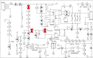
I am referring to the document number TIDA-00173 and to create a higher capacity (approximately 100W) flyback.

I'm configuring a flyback using UCC28711. (Refer to document number TIDA-00173)

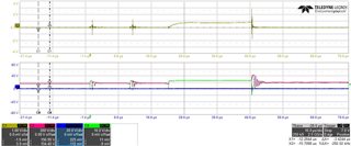
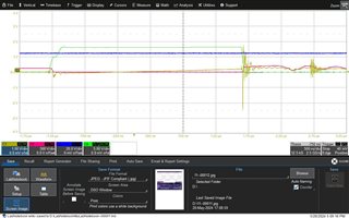
When pwm ic generating three initial pulses, I can observe momentary spikes in the value of CH1.(CH1: Vcs, CH2: VDS Q2, CH3:VDD, CH4:VGS)

(Datasheet specifies the rated value as 780mV, so i need to make it lower value. I think it can solve it using RC filter.)

To solve this problem, I changed the R23 resistor on the VCS pin from 1k to 4.6k, which resulted in higher peak values. But, in my opinion waveform is more than clear.

(1k is upper graph, 4.6k is down gragh)

I wonder if PWM ICs are affected by such momentary peak values? If they are, is it appropriate to continuously adjust the RC values like this?
  • Hi Seungpyo,

    Thank you for reaching out.

    First of all the spikes on the CS pin at turn off indicates there is sufficient parasitic capacitance, so we might have to ensure the Coss of the MOSEFT is optimal. If this voltage at CS pin is greater than the overcurrent protection threshold, the device will shutdown.

    The series resistor acts as a line compensation resistor, so increasing this value 3x helped startup because, the offset in current is high, but this could mean your actual current in the system could be lower which probably facilitated startup. Second thing might be to ensure is you want to probe the CS pin signal using tip and barrel measurement so as to ensure the oscillations are not due to probe pick up.

    Regards,

    Harish 

  • Thank you for your help. I am currently using the C2M1000170D FET from CREE. This product has a COSS value of 19pF, which is larger than the 9pF of the previous MOSFET.

    Additionally, since the converter is not working, I removed the upper switch and connected it directly to the line. As a result, there is currently only one MOSFET

    I measured the VCS voltage using a passive probe on an oscilloscope, keeping the probe lead length as short as possible (about 2cm or less).

    I am currently trying to reduce the spike in VCS. I have been continuously changing the resistance values of the CS pin and the shunt resistor, but the spike voltage still occurs. I tested the CS pin resistances with 3k and 4.5k, but the spike voltage did not change significantly. I also reduced the shunt resistance from 0.4 ohms to 0.2 ohms.

    Is there any way to solve this issue?

  • Thank you for your help. I am currently using the C2M1000170D FET from CREE. This product has a COSS value of 19pF, which is larger than the 9pF of the previous MOSFET.

    Additionally, since the converter is not working, I removed the upper switch and connected it directly to the line. As a result, there is currently only one MOSFET (see the attached photo).

    I measured the VCS voltage using a passive probe on an oscilloscope, keeping the probe lead length as short as possible (about 2cm or less).

    I am currently trying to reduce the spike in VCS. I have been continuously changing the resistance values of the CS pin and the shunt resistor, but the spike voltage still occurs. I tested the CS pin resistances with 3.3k and 4.5k, but the spike voltage did not change significantly. I also reduced the shunt resistance from 0.4 ohms to 0.2 ohms.

    Is there any way to solve this issue?

  • Hi Seungpyo,

    Thank you for reaching out.

    The switched node capacitance could be very high - cumulative effect of transformer, Coss & output rectifier relected cap. 680pf on the CS pin seems very high and it is generally advisible to keep this to less than 120pf. (220pf max). I think you can try using npn-pnp buffer on the gate to drive the SiC.

    Regards,

    Harish

  • Hello,

    Thank you as always for your prompt response.

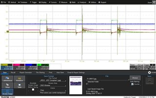
    As you mentioned, I changed it to 120pF (maximum 220pF), but during the operation test, I observed the following phenomenon at low voltage. I am writing to ask whether this is an abnormal operation or normal operation.

  • Hi Seungpyo

    The third pulse looks weird. The ON time appears long. It might be due to some delay on the Vcs signal or too high primary inductance or very low input startup voltage. Each of the above condition needs to be verified independently.

    Please let us know if you have further questions.

    Regards,

    Harish