Other Parts Discussed in Thread: TPSF12C1EVM-FILTER, TPSF12C1
Tool/software:
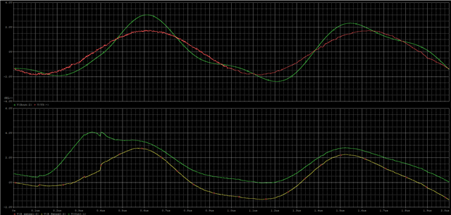
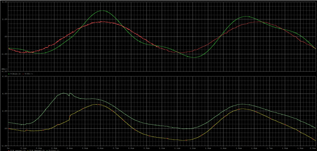
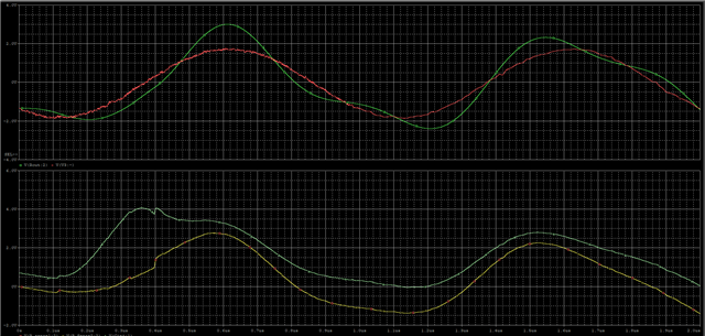
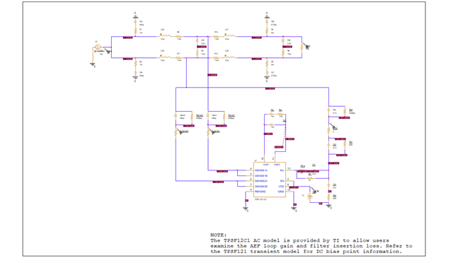
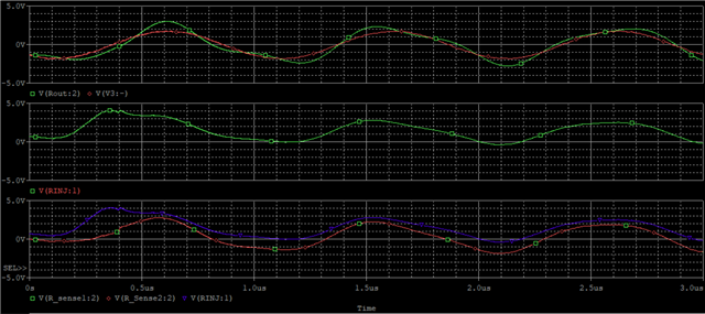
The circuit shown in PDF was built in Pspice for TI to check the noise reduction effect of the AEF.
In the simulation, a 1.0 MHz sine wave was used as common mode using the PWL (Piecewise Linear) function.The reason for not using a Sin voltage source was that the noise reduction effect could not be verified because of the noise generated by the ideal voltage source even if the AEF outputs an INJ.
Symbol;.
V(V3) : Input voltage (1.0MHz Sin-wave)
V(Rout) : Output voltage
V(RINJ) : AEF output voltage
V(Rsense1, Rsense2) : Input voltage of AEF (Noise detection)
The following questions.
From the simulation results, the voltage peak of the load voltage (common mode +AEF INJ) differs from the measured value due to an increase in the voltage peak of the load voltage (common mode +AEF INJ).
Is this a problem with the circuit construction or with the AEF Pspice model?
We consider it correct that the amplitude of the load voltage V(ROUT) approaches zero.
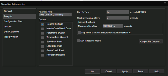
 Simulation model of TPSF12C1_Transient.pdf