Tool/software:
Hello:
Display no current and power PCB test record (1)
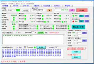
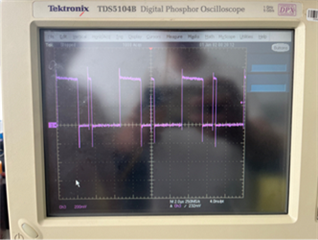
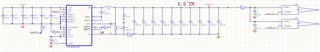
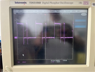
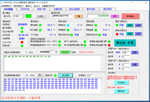
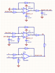
1. The abnormal device is powered on for measurement. After the pump is turned on, when the output power is 1W, the host computer displays that the pump output current is 0, and the circuit board makes a dripping sound. The waveform of the SW output pin of the DCDC chip LM61480 is measured as shown in the figure below, indicating a hiccup protection phenomenon.
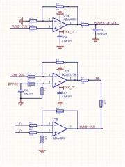
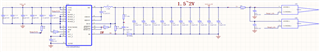
2. Measure the voltage at each position in the pump drive circuit and find that all devices at each position have abnormal test data as follows:
2.66V R5 2.39V R6 2.14V R25 1.90V R22 1.66V R27 0.841 R31 0.25V
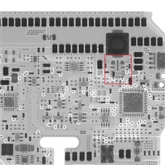
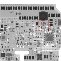
3. The U13 chip was irradiated with X-RAY and no welding short circuit was found.
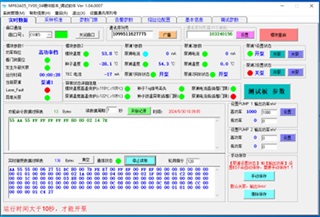
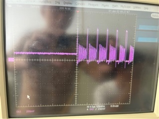
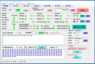
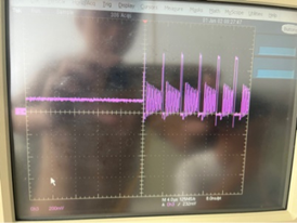
4. Remove the U13 power chip LM61480 and replace it with a new LM61480. When the pump is turned on and the output power is 1W, the upper computer displays a pump output current of 5.2A, which returns to normal. Test the waveform of the SW output pin of the DCDC chip as shown in the following figure.