


Other Parts Discussed in Thread: BQ24133
Tool/software:
Hello TI Engineers,
I would like your assistance with reviewing the layout of the TPS54821 circuit. This is a related to a previous post I made about introducing a reverse current protection to the buck converter. Here is a link to the previous question: https://e2e.ti.com/support/power-management-group/power-management/f/power-management-forum/1363426/tps54821-reverse-current-protection. The TPS54821 buck converter circuit is only a section of a larger mixed signal circuit design. I have only included the TPS54821 schematic and layout section of the main design in the attached file. (ZIP file for the GERBER and PDF for the schematic below). Let me know if you are able to open those files
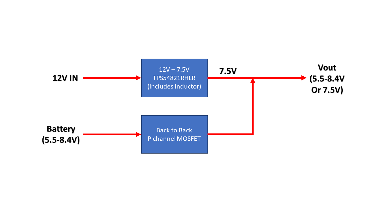
Below is the block diagram of the TPS54821 circuit followed by the schematic version of it. The 12V IN (Vcharger) is also connected to a charging IC for the Battery (VBAT). The Charger IC is a BQ24133 with power pathing MOSFETs. Because there are components that connect directly the 12V (Vcharger) node, we added a MOSFET before the input of the of the BUCK. This MOSFET is controlled by a microcontroller signal that also controls the Enable Pin of the Buck IC. The additional MOSFET was based on the suggestion of the TI Engineer from my previous post: https://www.ti.com/lit/an/slyt689/slyt689.pdf.
Block Diagram
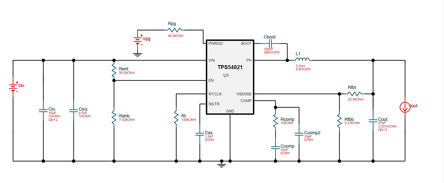
BUCK and Back to Back FET Schematic

TI WebBench Design
As previously mentioned the BUCK and Back to Back P Channel MOSFET are only powered one at a time. They will never be on simultaneously. The schematic and layout we have is based on a TI Web Bench design. The only modification we made in the schematic is connecting the Power Good Pin to ground since we do not use it. For the TOP layer, we followed the layout from Web Bench where PVIN and VIN are connected on the same Copper Polygon Pour. For Inner Layer 1, the layer below Top Layer, we copied the TPS54821 EVM, where it has a duplicate of the PVIN and VOUT copper polygon pour of the TOP layer. The Inner 2 Layer and Bottom Layer are mostly ground planes. In the gerber files, you would notice additional traces surrounding the BUCK Circuit. These are signal traces either connecting the the BUCK circuit (ENABLE PIN and Output Voltage going back to the feedback resistors) or the charging circuit which is located to the top of the BUCK circuit. These traces are mainly in the bottom layer. There are no PCB trace that go under main power/switching section of the BUCK layout. Let me know if you have any clarifications with the layout gerber files we have attached.
SCHEMATIC
TOP LAYER

INNER 1 (EVM)

Thanks,
Deniel
