This thread has been locked.

If you have a related question, please click the "Ask a related question" button in the top right corner. The newly created question will be automatically linked to this question.

UCC21755-Q1: Gate drive signal problem

Part Number: UCC21755-Q1

Tool/software:

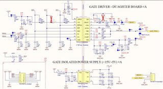
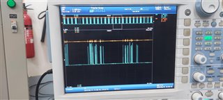
for the UCC21755-Q1, based gate driver, I am facing challenges as gate drive signal toggles in spite of input PWM signal remains steady. there are heavy ringing in the Vgs signal as shown in attached image. CH - 1 : Input PWM Signal; CH-2 : VGS waveform. Mosfet P/N is C3M0075120D.

I doubt, 1) DESAT Circuit; 2) Power Supply; 3) Layout

Please suggest troubleshooting options to this issues so that i can provide more waveforms for your reference. 

P.S.: there is bandwidth filter in input PWM signal. Please bear with the attached waveform. I will try to capture more accurate results by tomorrow. 

  • Hi Darshankumar,

    Can you add 100nF directly across VSS and VDD? Also, what does your high voltage bus look like? You might have a lot of parasitic resonance in the high-voltage switch node that you need to fix with decoupling and snubbing. What is the frequency of these noises?

    Best regards,

    Sean

  • Thanks Sean for your inputs.

    Hi Darshankumar,

    Thanks for the schematics and the scope capture. As Sean mentioned please add 100nF cap close to device across all the supply pins (VCC, VDD and VEE) and also increase the capacitor on the INP and INN pins to be 100pF. These changes will help.

    Please do share INP, Gate (Vgs) and Vds voltages if you still observe issue.

    Thanks

    Sasi

  • Thanks for the suggestion. there is already 100nF & 10uF cap across all supply pins as shown in schematic. I will also add 100nF between VDD and VEE as Sean Suggested. and increase INP and INN cap to 100pF.  I will  check and revert you back.

  • Hello Team,

    I updated capacitors and PWM input filter as per suggestion, However there is no improvement.

    Please consider below waveforms:

    1) Vgs (BLUE) Vs Vin+ (PWM input on IC)

    2) Vgs Vs 15V (VDD)

    3) Vgs Vs -5V (VEE)

    4) Vgs Vs VDSAT

    Please let me know if you've suggestions. 

  • Hi Darshankumar,

    It will be easy to capture all the Secondary signals together to understand the status of all the key signals at the same time. Also can you please label the waveforms in the plot so its easy to follow.

    I have assumed the plots based on your description.

    In plot3, I see Vgs is quite noisy even when PWM is just high (fixed - not switching). Do you know what is causing the noise in the system? (what other parallel operation happening during that noisy moment? )

    Also long cables (even probes) when connected through noisy environment act like antenna  and pickup noise.  Also probes to be connected with short ground loop. 

    Thanks

    Sasi

  • Yes, Sasi. the Plot3 is Vgs vs PWM. Strangely there is no mosfet switching operation is going on. we're just testing pulses on mosfet gate source without any DC link voltages by applying dummy pulses on gate driver board.

    Please allow me some time, I will capture the waveforms as requested and share it shortly.

  • Sure Looking forward for your system waveforms. As we have indicated before, please use twisted pairs of cables for PWM signals (if possible coax) to minimize noise into the system.

    Thanks

    Sasi