This thread has been locked.

If you have a related question, please click the "Ask a related question" button in the top right corner. The newly created question will be automatically linked to this question.

LM5181: Output Zener Diode role in a flyback circuit with LM5181-Q1 converter

Part Number: LM5181
Other Parts Discussed in Thread: LM5180

Tool/software:

Hi Ti Team, I want to use LM5181 in my application.

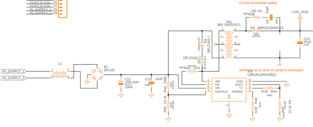
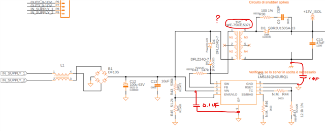
The  general specs are : Vin (10-40 VDC), Vout ISO (13V), Iout max < (0.1 A) 

Inserting these data into Webench I get a schematic with a zener diode in parallel with the output ,called Dzout.

I attach the screen of the schematic. In the BOM created by WeBench I don't find the value of the component..

Could you explain me the role of this zener diode in the circuit and its realistic value? 

I'd be grateful also If you describe me the calculations  you make to obtain Dzout value.. 

Thank you

Alessandro

  • Hi Alessandro,

    Thank you for posting.  Please also use our design calculator to help you design.

    https://www.ti.com/tool/download/LM5181DESIGN-CALC

    Regarding the output Zener, it is to help clamp the output voltage when your output becomes open.  The LM5181 has a min load requirement. 

    You can use a dummy load, or use a Zener, or both. The Zener voltage should be about 10% higher than your Vout setting voltage. 

    Between the dummy load and Zener:  the dummy load, although small, would cause permanent power loss.  The Zener will only conduct when your output load is less than the required min load.

    Hope this clarifies.

    Thanks

    Youhao

  • Hi Youhao,

    thank you for your clear answer.

    Basing on the following TI formula quoted in the attached link : "The minimum current delivered to the load is Iout-min = 0.5*Lmag*Ipk-FFM^2*Fsw-min/Vout, where Ipk in FFM is 0.3A and 0.15A for the LM5180 and LM5181 respectively, and Fsw-min is 12kHz" I obtain a  minimum current very low for my application : 0,7 mA.

    Also, I think that in my real circuit this minimum load will be granted in any cases.

    Do you think that in this situation is still useful to insert the zener diode?

    I attach also the flyback real schematic of my circuit.

    Thank you for your support,

    Alessandro

    https://e2e.ti.com/support/power-management-group/power-management/f/power-management-forum/920195/lm5180evm-s05-light-load-operation-and-transient-response/3405446?tisearch=e2e-sitesearch&keymatch=lm5181#3405446

  • Hi Alessandro,

    I would reserve the Zener position on the PCB in case it is needed in the future, and choose not to populate it for now. 

    Regarding your schematic,  I would add a 0.1uF bypass capacitor across VIN and GND, and a 1 to 2nF across the primary and secondary ground.   Please pay attention to the transformer selection. I checked the Wurth website, and your selection is not for flyback application.  Please refer to our design calculator to help determine a proper flyback transformer. 

    For you reference, the transformer used in our EVM may work, although it is for dual output but you just need to use one output winding: YA8916-BLD. You may find some thing equivalent from other vendors.

    Also, please refer to our EVM layout example when designing your PCB.

    Good luck in your project.

    Thanks,

    Youhao

  • Hi Youhao,

    I only see the answer now cause I was out from office, thank you for your clarification.

    Ok I'll search another transformer for my application; unfortunately I can't find the one you suggested (YA8916-BLD) on the usual suppliers. Ideally I'd like to have 1.1:1  Nps ratio (this is what I get from the calculations) and Lprimary>32 uH.

    If you have other suggested partnumber I'd be grateful.

    A question: which is the role of the capacitor across the two isolated grounds?

    It seems to me that this capacitor may convey the emc noise from the isolated "output" ground to the primary one..

    I'm not able to understand how It works.

    Thank you for your support

    Alessandro

  • Hi Alessandro,

    You may contact Coilcraft to get the samples of YA8916-BLD:  cust_service@coilcraft.com.

    The turns ration 1.1 : 1 is a suggestion and the 1:1 transformer should work. 

    Regarding the 1nF capacitor across the isolation boundary:  It is to contain the common node noise by providing a return path back to the secondary.  There is common noise passing from the secondary to the primary via transformer winding capacitance (usually in scale of pF).  Reserve a capacitor there in case you need it after test.

    Hope this clarifies. 

    Youhao