This thread has been locked.

If you have a related question, please click the "Ask a related question" button in the top right corner. The newly created question will be automatically linked to this question.

TPS548A29: Schematic and Layout Review (failing part, shorting to ground)

Part Number: TPS548A29

Tool/software:

Hello, We have been having issues with our boards and the DC Reg (TPS548A29RWWR) shorting to ground through Vin/SW.

- Input is 11-14V; Output is 5.1V, 10A max (initial thought was we needed 7-10A, but we now only need 2A so this could be changed)

- Our goal was efficiency over size, so design uses 600kHz sw frequency. 

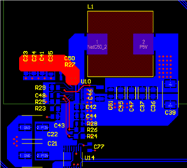
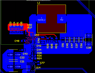
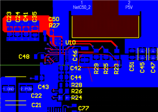
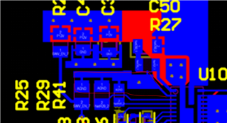
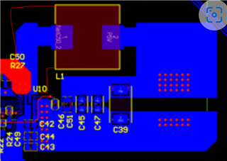
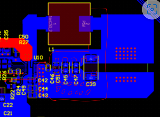
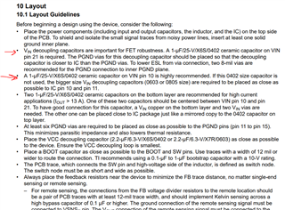
Reading through the forum here, we found that the common issues for this series was either layout or transient voltage spikes. We checked our layout, and added Elect-Alum caps to the input to help dampen anything that might be sneaking through, as well as increased the output capacitance. Further up the line, there is a TVS diode with a max clamp of 24.4V (SMCJ15A) on the input. We based these choices on the EVM schematics. 

Reading the datasheet deeper I believe I read the VCC capacitance (section 7.3.1) as "at least 2.2uF"  instead of correctly "at least 6V rating" on the VCC pin. Down below in the design example though (section 8.2.2.9) it says minimum of 2.2uF. Any issues here?

- 1st iteration was more stable, in that it would pass all tests in the lab but has been failing in the field.

- It seems that our 2nd iteration is less stable than the first, and fails much easier even in the lab.

Sch_Initial_Design_TPS548A29_5Vout.png

Layout_Updated_Design_TPS548A29_5Vout.png

Sch_Updated_Design_TPS548A29_5Vout.png

  • Updated schematic files (pdf versions)

    sch-updated.pdf

    sch-original.pdf

  • Hi Zach, 
    The VCC capacitance should be 2.2 uF with at least 6.3 V rating. Looking at the schematic, the AGND and PGND connections need to be separate and have different symbols. EN, Mode, and Trip are noise sensitive and should be connected to AGND. There should be a separate AGND pour and have it connected at a single point to a solid PGND plane on an inner layer. Also, a 220- pF CFF is required for this design. I would recommend decreasing your Rtrip resistor to 5.76 k for 10 A valley current limit. However, if you only need 2 A and want to lower your overcurrent protection you can increase your Rtrip resistor to 11.3 k for 3 A valley OCP. I didn't see a PGOOD connection on the schematic and it should be pulled up to VCC with a 1k-100k resistor. 

    Best,

    Ryan

  • Great, thank you. 

    How does the updated layout look then? I've shifted the output capacitors over to put the TRIP and EN resistors next to C46 (VCC) and added the AGND which direct connects to solid PGND on plane below.

    Also, do you see any issues with the input/output capacitance (before or current)?

    How would I determine on my own that a 220pF CFF is required?


  • Hi Zach, 

    The input/output capacitors look okay. 
    Is this the AGND plane? How does it connect to the AGND pin?

    We have a design calculator on the web that you can use to enter schematic values and it will provide feedback:


    Best,

    Ryan

  • Hi Ryan,

    Thanks for your quick response here. It's been very useful and helped point me to the right area for tools you provide. I've attached the updated schematics, where I've swapped to 800kHz switching and included the new 220pF Cff (based on the design spreadsheet it should remain 220pF). I've also updated the layout images with close-ups of the different areas. AGRND connects to GND on the inner plane. I think we are all good now, but would love any additional review.

    Typically i would place components on the top/bottom layers, but we have another piece that mounts flush with the top so we can only route traces there, no components. 

    sch_2D00_p5v_2D00_pwr.pdf

    new_2D00_layout_2D00_agnd.png

    new_2D00_layout_2D00_feedback.png

    new_2D00_layout_2D00_full.png

  • Hi Zach, 

    The schematic looks okay. Regarding the schematic, I would recommend to connect AGND components with a larger pour like this:

    I would also recommend increasing the width of the traces SW. 


    VOUT trace should be wide but also short with the output capacitors close to the output of inductor with the vias shortly after the output capacitors:

    Here are some other layout recommendations from the datasheet:

    Best,

    Ryan