This thread has been locked.

If you have a related question, please click the "Ask a related question" button in the top right corner. The newly created question will be automatically linked to this question.

UCC28951: Ringing at output during series connection.

Part Number: UCC28951

Tool/software:

Hi Mike,

Schematic is reviewed by you which was shared to you by Nihil. 

Vin: 280VDC

Load : 26V regulated, 10A

Transformer primary inductance: 2mH

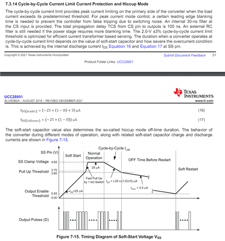
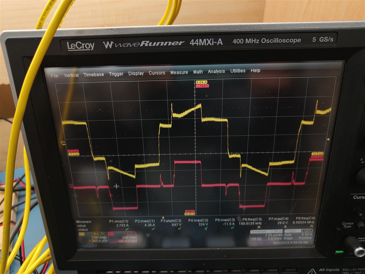
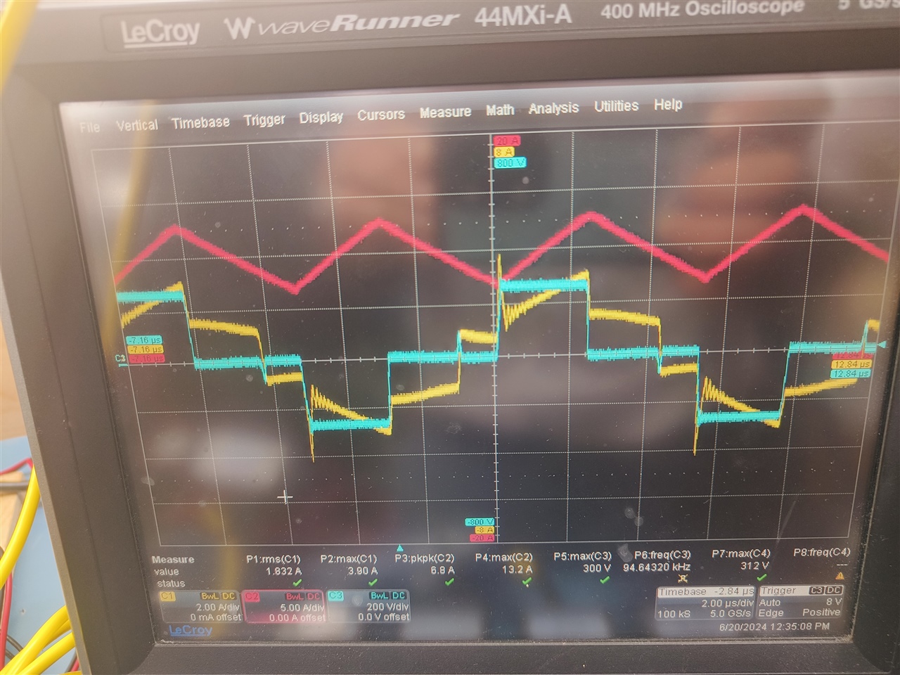
1. Below are the primary current waveforms, 

Along with inductor current. Are they correct ? Why the initial peak in current?

Yellow: primary current 

Red: inductor current 

Blue: transformer primary 

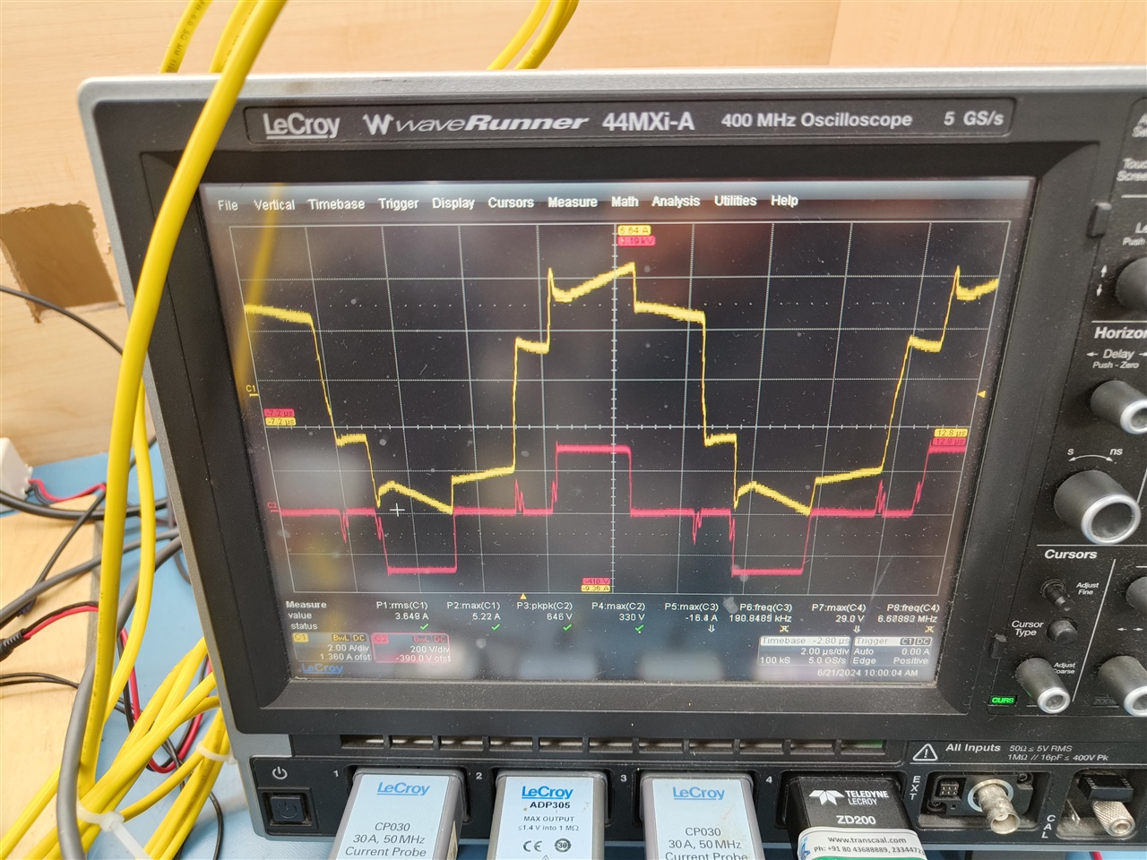
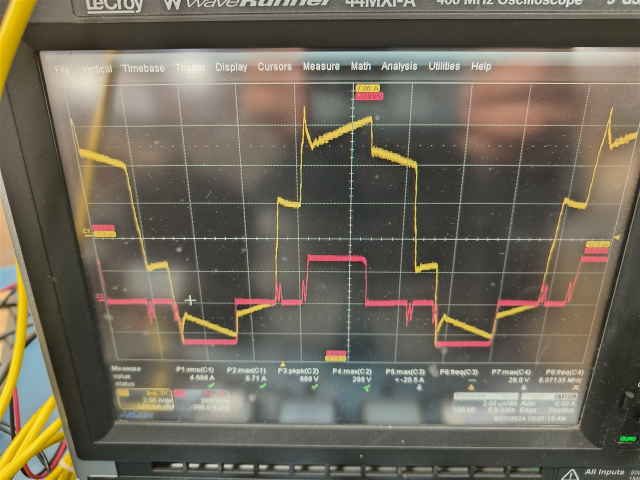
2. Output voltage waveform with ringing. The outputs are connected in series winding, regulated to 24V. 

Blue: output voltage 

Yellow: primary current 

Green : primary gate B

Though compensation is still in progress, I tried adding higher SRF capacitors by measuring the ripple frequency ( 6 Mhz ) and also tried increasing output inductance, still that ringing didn't change. Inductor waveforms also looks clean from waveforms. Till it enters inductor I don't see any ringing. 

That ringing increases with increase in load current. 

One more thing which I noticed is bottom winding ( vout 2 ) didn't have ringing, only minor spikes. Tomo plan is to check both windings seperately and check whether interwinding capacitance at secondary is trouble or primary side transformer coupling capacitance is trouble ? 

I WILL also check both winding seperately.

Compensation values @ present:

Cz:6.8nF

Rz: 51K

Cp: 680pF

Rsum : 91K

Your thoughts and advise ??

  • Hello,

    1.  In regards to the waveforms in scope plot 1  they look as expected, except the large spike in current when the design comes out of freewheeling.

    This could be due to your SR timing being off.  You might want to double the SR timing to make sure it is not causing this leading edge current spike.

    2. The following link will bring you to an excel design that use to set/check your voltage lop compensation.  The excel tool uses the same equations as what is presented in application note SLUA560.

    https://dr-download.ti.com/design-tools-simulation/calculation-tool/MD-rlvLC7vkDZ/01.00.00.0D/sluc222d.zip

    https://www.ti.com/lit/pdf/slua560

    Please note that the excel tool and calculations need to be verified with a network analyzer to check stability.

    3.  Your waveforms seem to have a constant duty cycle.  So these oscitations may not be do to loop instability.  They could be caused by trace inductance, transformer and output leakage inductance.  If this is the case you may be able to the fix the issue with one or all of the following.

    a.) R C snubber across the output rectifiers R = (L/C)^0.5.  I set C to (1/fsw)*(0.02/(3*R).

    b.) Some designer use R C snubber across the shim inductor as well.

    c.) If the snubber does not work your trace lengths in your power stage might be to long.  Consider relaying out the board to reduce trace inductance. 

    d.) There might be too much leakage inductance in your inductor and transformer. You can reduce this by selecting magnetics with less leakage inductance.

    Regards,

  • Ok, let me try these and get back to you.

    Q1.

    With regards to point 1,

    At present there is no shim inductor and freewheeling diodes ? Should I put back just diodes or shim as well ?

    Additionally DELAB :51k, DELEF : around 30K, I read somewhere DELEF should be halve of DELAB, as per your suggestion should I double DELEF ??

    Q2.

    Also please do explain a little more on points C and D

    c.) If the snubber does not work your trace lengths in your power stage might be to long. Consider relaying out the board to reduce trace inductance. Should I connect transformer and FETs external to board and check ?? 

    d.) There might be too much leakage inductance in your inductor and transformer. You can reduce this by selecting magnetics with less leakage inductance.

    Q3: at present I'm not able to go more than Vin :300V, load :10A , transformer starts to make some audible noise , duty cycle and starts to vary,  I understand this might be due to loop compensation? Any suggestions here ? Present components values are as mentioned above. 

    Q4: there was a scenario, Vin : 300VDC, LOad current more than 10A, controller was shutting down. Was it hitting any limit ? FYI, at low voltage around vin:  200V , I have gone upto 15A. Any thoughts here ??

  • Hello,

    Please see my comments below.

    Q1.

    With regards to point 1,

    At present there is no shim inductor and freewheeling diodes ? Should I put back just diodes or shim as well ?

    > When the primary is shorted with A and C, B and D the design is freewheeling.  If you are using FETs to replace diodes that is O.K.  The UCC28951 was actually designed to this.

    > The shim inductor is used to achieve ZVS.  However, if your leakage inductance is large enough you might not need it.

    Additionally DELAB :51k, DELEF : around 30K, I read somewhere DELEF should be halve of DELAB, as per your suggestion should I double DELEF ??

    >What you need to make sure is that the SRs are not shorting out the transformer primary when A and D FETs are on or C and B FETs are on.  I thought this might be happening due to that large current spike when you come out of the freewheeling time.

    Q2.

    Also please do explain a little more on points C and D

    c.) If the snubber does not work your trace lengths in your power stage might be to long. Consider relaying out the board to reduce trace inductance. Should I connect transformer and FETs external to board and check ?? 

    > You should study your layout to see if you have traces adding inductance.  These would be long traces.  1 inch, 2.54 cm, of trace adds 10 nH of inductance.  10 inches, 25.4 CM would add a 100 nH of inductance.  Please note I don't think your layout is this bad, this is just an example.  The shorter the trace length the better.

    d.) There might be too much leakage inductance in your inductor and transformer. You can reduce this by selecting magnetics with less leakage inductance.

    >You can do this by reviewing magnetics data sheets and selecting different components.

    Q3: at present I'm not able to go more than Vin :300V, load :10A , transformer starts to make some audible noise , duty cycle and starts to vary,  I understand this might be due to loop compensation? Any suggestions here ? Present components values are as mentioned above. 

    >Check your loop compensation with the excel tool and application note.

    Q4: there was a scenario, Vin : 300VDC, LOad current more than 10A, controller was shutting down. Was it hitting any limit ? FYI, at low voltage around vin:  200V , I have gone upto 15A. Any thoughts here ??

    >If you are hitting cycle by cycle current limit of 2 V to long the controller will shutdown and reactivate soft start.   This is known as over current hiccup mode protection is described below.


    >Your transformer current is showing excessive current and the cycle by cycle current limit is protecting your FETs.  You need to figure out what is causing this excessive current and correct it.  My guess is that your SRs are on when they should not be.  Please note the tool estimates the timing setting for ADELEF.  You need to verify and adjust based on actual circuit performance.

    Regards,

  • Below are today's test results.

    FYI, ADAPTIVE delays have been shorted to ground. 

    Added resonant inductor 10uH, freewheeling diodes, I'm able to load upto 26Amps.

    Below waveforms for 5A, Vin : 270VDC

    Below waveforms for 15A, Vin : 270VDC

    Below waveforms for 20A, Vin : 270VDC

    Below waveforms for 25A, Vin : 270VDC

    Going beyond 26A, it's shutting down, maybe since it's hitting over current limit. Additionally I did increase DELEF from 24k to 47K as you said , but no change is observed.

    What I also noticed output side ringing stays same in amplitude with increasing current from 10A to 25A. My understanding is primary side current peak issue is  different and ringing at secondary is different. Still not worked on snubber circuit as I was focussing on primary current peak. 

    Is there any significance change in primary side current ? What is happening? Please explain and how do I go forward ? 

  • Hello,

    I am reviewing your inquiry and will get back to you shortly.

    Regards,

  • Hello,

    It seems that the changes you made have reduced the ringing that was seen on the transformer primary current.

    It also looks like you are getting more current out of the design so it seems like you making progress.

    You increased the delay time on the E F FET turn on delay and it did not remove the CS spike on the transformer primary current.

    So this may not be the cause of the issue.  However, you might want to study the gates of the SR FETs with the primary current of the transformer just to make sure these FETs are not the cause.

    I do believe the leading edge current spike on the transformers primary current when coming out of freewheeling is preventing you from achieving full power in your design.  If you can remove this spike the design will behave better.

    You might want to check the gate of the FETs compared to the transformer primary current to see if the timing the FETs is correct.  If you turn on the H Bridge FETs on to early this could cause a current spike in the transformer primary current.  di =V*dt/L  You want to turn the FETs on at the bottom of the resonant ring at the switch nodes.  You can set the delay timings of the H Bridge FETs at 10% load.

    I will be on vacation for the next two weeks.  If you need help with this over the next two weeks please contact Nihil.  If you still need help in the future, please repost in the e2e.

    Regards,

    Nihil