This thread has been locked.

If you have a related question, please click the "Ask a related question" button in the top right corner. The newly created question will be automatically linked to this question.

TPS2116: Reverse current protection activation with LM66100 LDO with active discharge

Part Number: TPS2116
Other Parts Discussed in Thread: LM66100, , TPS7A03

Tool/software:

Hello everyone,

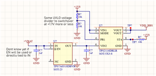
I am currently designing a battery backed supply for a MCU. There is a primary voltage source which supplies power to the MCU in normal operation. Once it falls, a coin cell (240 mAh, 3V) powers the MCU in a low power mode. The thing is that the coin cell voltage can't be directly applied to the MCU because the max voltage of MCU power pin is 1.9V. Of course reverse current blocking is a must in this circuit. In order to achieve this design requirement, I have designed the following (it is just an idea):

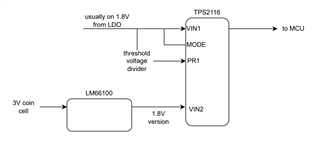
So, in normal operation the usually on LDO powers the MCU because of the MODE pin. My question come after having read the following post: [FAQ] TPS2117: Why isn’t my Power Mux blocking reverse current/voltage? - Power management forum - Power management - TI E2E support forums

It says if no pull down circuit is available in VINx pins VOUT may pull VINx to its voltage. This is no problem for VIN1 as there is already a voltage divider connected to it. But I don't want to connect a pull down resistor to VIN2 as it will consume the coin cell when it powers the MCU. I am worried if this may damage the LM66100 IC itself.

I have noticed that there is a version of LM66100 with active discharge, that is actived when the IC is not enabled or UVLO condition happens.

Is it the P version of LM66100 enough to avoid backpowering or unwanted current or will the version without this feature work anyway? Is necessary to shutdown the LM66100 to active discharge happen or is this also available when the EN is H (imagine that the Iq current is tolerable and don't want extra components to drive the EN pin in order to achive the shutdown current).

Of course if more suitable components are available for this case, please let me know.

Please correct me if there is a misunderstanding in my post.

Best regards,

Gorka.

  • Hi Gorka,

    First, how is 3V voltage from the coin battery being brought down to 1.8V ? The LM66100 device is an ideal diode and not an LDO, and it doesn't have the ability to buck voltage. I would recommend a buck converter or an LDO here, and some buck converters even offer reverse current protection. Also the TPS2116 does have some reverse current blocking ability.

    I'm not sure how to answer your question regarding the resistor to ground at the V_in2 pin, but I'll reach out to the author of that FAQ post to see if this is relevant.

    Best regards,

    Nate

  • Hi Nate,

    I wrote the LDO name wrong, I meant TPS7A03 which has a very low Iq and a low minimum input voltage. I was considering different ways to implement the switchover and I was also considering two LM66100 instead of  a single TPS2116, but I finally decided to use the last one because of the priority feature.

    When you get an answer from the author of the article please let me know.

    Best regards,

    Gorka.

  • Hi Gorka,

    The author of the app note will be available next week and I'll check with them as soon as possible on Monday. Just for clarity, can you send an updated version of the image from your original question? It sounds like you've made some changes and I'd like to understand exactly how they would appear.

    Thanks,
    Nate

  • Hi Nate,

    Sorry for the delay. I have updated it and made a preliminary schematic. You can look at it right below:

    The use case is as follows,  power VDD_BBS with +1V8 in normal operation, once it falls below some threshold (say +1V7, it will depende on UVLO voltage divider at PR1) it switchovers from +1V8 to  LDO porwered by +VBATT. The question is if this circuit will work or if there is any issue at discharging or any other problem.

    Best regards,

    Gorka.

  • Hi Gorka,

    We had a look at your schematic and we don't see any issue with this setup. There's no concern of voltage from one channel affecting the other, and there's no reason to be concerned about reverse current unless you're planning to add additional voltage supplies to V_out.

    Best regards,

    Nate