


Background
When designing a power path with two or more input sources, it is imperative to not only be able to decide when to switch from one input to another, but also block current flowing from the active source to the inactive source in order to prevent shorting between inputs or unnecessary current consumption when power draw is a scrutinized resource. Furthermore, in order to protect upstream components and sources from overvoltage conditions or excessive current sinking, it must be ensured that any voltage sources on the output – whether they are intended or unintended – do not source current to the input sources.
This is where TI Power Muxes’ Reverse Current Blocking (RCB) feature shines – devices including TPS2121, TPS2116, TPS2117, and more can independently block current flowing from the output to the input on an inactive channel, on both channels if VOUT > VINx (active source, referred to as VINx), or if manually selected to do so. These devices protect input sources from higher voltages or shorts on the output by blocking reverse current if the output voltage is a certain amount higher than the input voltage – for example, TPS2117 will activate RCB if VOUT is 42mV (typical) greater than VINx.
Issue
However, some designers might find themselves in a situation where even though VOUT has a voltage source or a high capacitance on it and VINx is not being powered, RCB does not activate and VOUT pulls VINx to its voltage. This is likely because VINx is floating or has a low conductance path to ground such that it can be considered floating, which can be caused by an unconnected input, a voltage source that cannot sink current, or an improperly soldered component.
If VINx is floating or has a high resistance to GND, it is essentially an open circuit from the perspective of the Power Mux and VOUT net, and there isn’t enough current to enforce a substantial voltage difference between VOUT and VINx. The Power Mux sees this situation the same as when VINx is powering VOUT with no load – in both cases the voltage drop across the VINx FET is very close to 0V and the device will continue conducting between VINx and VOUT.
What can I do about it?
For example, say we have TPS2117 in a radio-enabled data-collection system. The system has three operating states: a high-power mode for transmitting data over radio, a medium-power mode for powering an MCU, sensors, and flash memory, and a low-power mode that powers critical sensors and only wakes the MCU if there is a significant data event. The system uses a single 3.4V lithium-ion battery.
|
VIN1 |
3.3V |
|
CIN1 |
100uF |
|
VIN2 |
1.8V |
|
CIN2 |
100uF |
|
COUT |
300uF |
The system is set up as described in Figure 1:
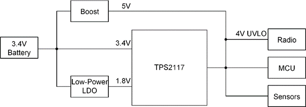
When the system switches from the medium-power mode to the high-power mode, the battery keeps the TPS2117 IN1 at 3.4V while the boost brings the output to 5V, and the device’s RCB quickly activates. However, when the system switches to the high-power mode from the low-power mode, problems can arise as most LDOs cannot sink current. In this scenario, there would be 5V on the LDO output, which can damage it as most low-voltage LDOs have an absolute maximum voltage of 4.1V. Thus, measures need to be taken in order to force RCB’s activation in this state. Some options are:
- Choose an LDO with a higher voltage rating. This can add more cost to the system and other specifications can suffer as a result.
- Choose an LDO with OV shutoff and integrated output discharge. This can add more cost to the system, but may cost less and have better specifications than a higher-voltage LDO.
- Place a FET that has a threshold voltage greater than 1.8V and less than 5V between the LDO output and ground. This will pull the IN2 pin to ground and activate RCB when the 5V boost is activated.
- Increase the capacitance on IN2. This may keep IN2 low enough while charging the capacitance for RCB to activate.
- Find another way to ensure that IN2 has a clear pulldown, either to the active input voltage or ground.
- Post a new question on the e2e forums by clicking the red button in the top right of the page.
Happy designing!
