This thread has been locked.

If you have a related question, please click the "Ask a related question" button in the top right corner. The newly created question will be automatically linked to this question.

UCC27212A-Q1: gate driver with single input and dual output

Part Number: UCC27212A-Q1
Other Parts Discussed in Thread: TPS28225-Q1, , UCC27712-Q1, UCC27714, UCC2897A, UCC57108-Q1, UCC27444-Q1, UCC21551-Q1, UCC21551, UCC23525, UCC21530-Q1, UCC21530, UCC21330, UCC28C53-Q1, UCC27624, SN6501

Tool/software:

 Hello Ti Team,

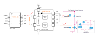
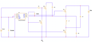
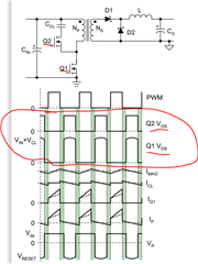
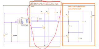
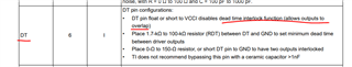
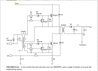
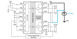
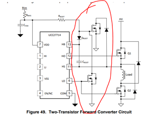
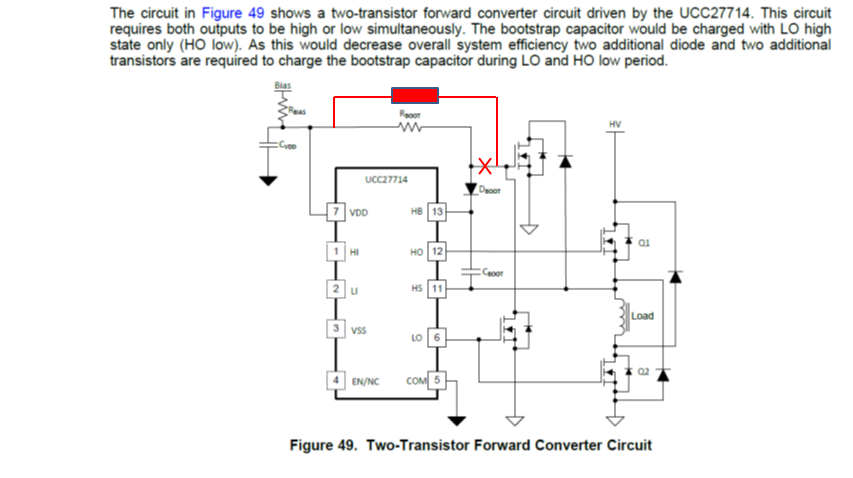
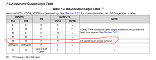
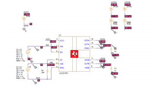
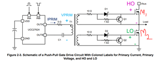
I am looking for half bridge gate driver with single input(IN) and two outputs (OUTA,OUTB)..I will be using for two switch forward converter which drives the two MOSFETS at the same time .

So single input and two outputs (OUTA,OUTB) which drives the high and low side MOSFETS.

and the driver should be AEC-Q automotive qualified....

Please check and let me know suitable gate driver

Thanks,

karthik

  • Hey Karthik,

    Thank you for reaching out to TI with your question regarding our half-bridge gate driver portfolio.

    The only Automotive qualified half-bridge driver that is in our portfolio currently is the TPS28225-Q1. It is a 4A driver and is 27V rated. What is your bus voltage?

    Another option is to use a product like the UCC27212A-Q1 and implement an inverter circuit to use 1 PWM signal for both the HI and LI inputs.

    Let me know if you have any questions.

    Thank you,

    William Moore

  • Hi William,

    Ok then i will use controller+  UCC27212A-Q1 half bridge driver which drives the two switch forward converter.

    Your statement  "implement an inverter circuit to use 1 PWM signal for both the HI and LI inputs"  ==> invert circuit is not necessary William because both MOSFETS of two switch forward converter should turn -on at the same time.

    So 1 PWM signal to diive Hi,Li  inputs of the driver sufficient i think so..like below picture.

    I will go like above picture shown i think it could be ok..what is your opinion william??

    Thanks,

    Karthik

  • Hey Karthik,

    Thank you for the explanation and diagram. I better understand your use case now. Yes, you can use the UCC27212A-Q1 with a single input on HI and LI.

    With your current setup, the HO FET does not have the reference that it needs for Vgs that it would typically have with HS in a typical half-bridge circuit. Also, there is not a way to supply and recharge the bootstrap capacitor. I have made a quick model to show how this could be implemented. There is an example of this shown in the UCC27714 datasheet in Section 7.4.3 Operation with HO and LO Outputs High Simultaneously in Figure 49. This is not the same as how you would implement it with the UCC27712A-Q1. The UCC27712-Q1 has an integrated bootstrap diode and the MOSFET labeled M3 below is not connected to HB.

    As a disclaimer, this does not include all required components such as gate resistors and support circuitry. This shows the main components that are needed.

    Let me know if there are any questions.

    Thank you,

    William Moore

  • Thanks William for drawing  the the circuit.i got your point now ..as both switches of two switch  forward converter operating at the same time cboot cannot be charged without the external bootstrap circuit which you mentioned in the diagram and i have the ucc27714 datasheet figure 49.i understood you point.

    But i did'nt understood the bootstrap circuit operation...can you explain me in detail..

  • Hey Karthik,

    1. This circuitry with R1, M3, M4, and D3 is for biasing the high-side as you mentioned. So, when the HO/LO is off, M4 is now off which turns on M3 due to the gate no longer being connected to ground via M4. When this is the case with M3 on and M4 off, D3 now clamps the HS node to ground through M3 which allows the bootstrap capacitor Cboot to be charged and then it will be discharged when HO/LO is turned back on to drive the gate of M1.

    2. I am not sure which E2E thread that comment from Richard came from, but it appears that they are switching HO and LO independently and at opposite times, not at the same time. This would perform the normal bootstrapping operation with the exception of the charging path would include the inductor.

    For an alternative solution, you must find a way to bias the high side due to the typical bootstrapping operation will not work in this scenario. An isolated bias for HB-HS would be a possible solution that would no involve adding too many extra components. Check out this FAQ outlining some high side biasing solutions.

    [FAQ] How to bias the high side of a half-bridge gate driver and why

    Let me know if there are any further questions.

    Thank you,

    William Moore

  • Ok thanks you so much William for the great explanation.I had one more query ,need your suggestion on it!

    After doing some tradestudy on two switch forward and active clamp forward converter .I observed Active clamp forward gives better efficiency .

     Active clamp forward converter suits my application and gives better efficiency compared to two switch forward converter.So i am considering  active clamp forward converter in my design.

     We have to use only Automotive qualified AEC-Q components in our designs or projects  due to some constraints.

    UCC2897A fits my requirement but it is not AEC-Q qualified and i have checked there is no AEC-Q  qualified  active clamp forward converter  controller in TI.

    So my doubt is now,

    is there any option to go with Ti normal  PWM Controller + Ti Half bridge driver which can drive the active clamp highside forward converter operation.

    As two MOSFETS operate complimentary in active clamp forward converter ,with  general Half bridge driver can we drive it or is there any limitation to Active clamp forward converter?

    is there any Ti normal  PWM Controller + Ti Half bridge driver,  what is your suggestion please check and let me know William.

    Waiting for your reply!! Thanks in Advance!

  • Hey Karthik,

    I'm glad to hear that your design and converter are working effectively.

    As for a controller, I am the Applications Engineer for gate drivers so I am not the expert to comment on the best controller for you. In order to find that, it would be best if you started a thread with our controllers team.

    For using a half-bridge gate driver in the topology shown in that schematic, that is the intended operation for half-bridge gate drivers where Q2 and Q1 operate complimentary of each other (with some deadtime). This allows for the bootstrapping to occur and doesn't create a shoot through condition.

    For the circled waveforms, When Q2 gate is given a high signal (Q1 gate will get a low signal), the drain of Q1 will then be connected to the high voltage bus and Vds will be high. Then, when Q2 is low and Q1 is high in the complimentary portion of the waveform, Q1 Vds will now be low. This is expected operation for a typical half bridge setup.

    Let me know if you have any further questions.

    Thank you,

    William Moore

  • Hello Willam,

    Thanks for explaining the circuit.

    Question 2:

    Also Is there any any limitation to the bootstrap capacitor charging when i go for high frequency operation of the converter around 250khz ?

    Is there any application note for the calculation 

  • Hey Karthik,

    1. You are correct. You cannot use the UCC27212A-Q1 with a 280V bus voltage. For a driver that can withstand a 300V bus and does not have interlock, the only thing in our portfolio is the UCC27714. It is not automotive qualified as you have requested though. Another option is to use a low-side driver with a pulse transformer to withstand the high voltage and avoid the interlock requirement. Please take a look at this Application Note regarding pulse transformers.

    Why use a Gate Drive Transformer?

    2. For charging the bootstrap capacitor initially on startup, there will be a delay before the high-side (HO) outputs because HB UVLO must be satisfied. This charging occurs while the low-side LO is on and so it may take multiple LO pulses to charge the bootstrap capacitor initially. During steady state operation, LO will have to pulse enough to keep the capacitor charged to continue driving the high-side. Bootstrap capacitor sizing is calculated with this table to help optimize this process.

    [FAQ] UCC27282: How to Correctly Size the Bootstrap Capacitor for Half-Bridge Gate Drivers

    Let me know if there are any further questions.

    Thank you,

    William Moore

  • Hello William,

    Also thanks for suggesting  solution to it with recommending low-side driver with a pulse transformer.

  • Hey Karthik,

    1. Yes, I see how this may not work for your application. There are ways to use a low-side driver as a high-side driver using some methods of isolation. These are discussed in the FAQ below. We offer a variety of low-side drivers that are automotive rated such as the UCC57108-Q1 single channel driver or the UCC27444-Q1 dual channel driver. Another option would be to use a dual channel isolated gate driver like the UCC21551-Q1.

    [FAQ] UCC27624: Can I use a Low Side driver as a High Side driver?

    2. The pulse transformer current is dependent on the gate driver current output. With our low-side portfolio, we have source and sink current ratings of up to 10A. We have higher current isolated gate drivers as well.

    3. With this diagram that you have shown, there is no path to ground shown for charging the bootstrap capacitor. For this to work, something on the "TO LOAD" side would need to provide a path to ground for the bootstrap capacitor to charge. So as shown, this will not work for your application.

    With the requirement for an Automotive rated component without interlock and at least 300V rated, either an isolated gate driver or a low-side driver with the isolated supply solution as seen in the linked FAQ seems to be your best option.

    Let me know if there are any further questions.

    Thank you,

    William Moore

  • Hello William,

    Thanks for your lovely suggestion,

    I checked the UCC21551-Q1 it suits my requirement i think, but some doubts to confirm it.

    Question 1:

    I checked the datasheet ,if DT pin left open or floating overloap is allowed which i can use for two-switch forward converter for both mosfets driving same time. can you confirm it it is ok?

  • Hey Karthik,

    As a note, I realized that for the pulse transformer solution you can flip the polarity of the low-side secondary winding to achieve both outputs operating at the same time. See the image below:

    For your questions regarding the UCC21551-Q1, I am going to connect you with one of our isolated gate drivers applications engineers as they are the experts on that product.

    Thank you,

    William Moore

  • Hi Karthik, 

    1. Yes, you can disable the deadtime function by tying DT to VCC. This will allow the outputs to overlap.

    2. Your understanding is about right. The UCC21551 has an internal DC working voltage of Viowm=2121V. However, the channel to channel spacing will set a limit to the voltage that can be applied between them in open air without arching. The 3.2mm distance according to IEC60664 is only safe for 1000Vrms, when the pollution degree is 1 and the material grade is 1, as for this device. You can boost this by using a conformal coating, but for higher voltages it is usually recommended to use two, single channel drivers such as UCC23525.

    Best regards,

    Sean

  • Hello William,

    Thankyou,correct, we can do like below,

  • Hey Karthik,

    As it appears you have two potential solutions with either an isolated gate driver or the pulse transformer for your two-switch forward converter. I am going to mark this thread as resolved.

    Thank you,

    William Moore

  • Hello William,

    For the below question, Sean cashin not replied yet.can he clarify this query also

    Question :

    Can i power-up VDDA,VDDB with the same power supply (12v supply ) which has common ground GND??

    (OR) VDDA,VDDB should be powered-up with two different power supply which has two separate grounds isolated(GND1,GND2 in picture below) 

    Also if i give isolated supply like above, bootstrap circuit Cboot  is not required know ???

    isolated supply will drive high side MOSFET with constant supply to VDDA.

    question 2:

    I dont want primary to secondary isolation, can i connect GND pin to VSSB pin like mentioned below,. Is there any problem can you check and tell me..

    please clarify this  both query, thank you.

  • Hi Karthik,

    1. You usually cannot power both the output A and output B channels with the same 12V supply, since in a forward converter you need to drive a half-bridge. The high-side channel will require a bootstrap circuit or its own isolated supply, like in your second image. Could you maybe provide an overall power supply schematic? I am confused.

    2. You can connect GND and VSSB if you do not need isolation, but this should not be necessary if you have an isolated power supply on the output side. Isolation is usually a system-level benefit.

    Best regards,

    Sean

  • Hi Sean,

    The below picture is from UCC21551-Q1 datasheet first page.In the diagram they used same VDD supply to high side and low side which means they referred to same ground.

    so when output A and output B channels are powered up with the same VDD supply,Cboot and bootstrap circuit is required. Can you confirm this??

    Anyways i will use below mentioned external circuit to charge the cboot capacitor in two switch forward converter as both MOSFETS will turn-on at the same time.

  • Hi Karthik,

    1. Yes, you can use an isolated supply instead of a bootstrap circuit.

    2. This datasheet image shows a "bootstrap" circuit. It might not work in your circuit if the low-side switch is open. Your external circuit is a good idea if you do not use an isolated bias supply.

    Best regards,

    Sean 

  • Hey Karthik,

    As Sean mentioned, for the UCC27714 datasheet image, the thermal and current spikes through the bootstrap resistor would be very large due to the small nature of that resistance. So adding another larger resistor for that path would be advised as seen by the below image.

    Let us know if there are any further questions.

    Thank you,

    William Moore

  • Dear William and Sean,

    Thank you so much for your suggestions for the doubts which i asked.

    I am going to select the UCC21551-Q1 isolated half bridge driver. For further points or doubts in any i will contact you during design.Please share your both email id's in personal chat and also wanted to connect with you due the nice suggestion and discussion which you given. 

     Thanks,

    Karthik

  • Hello William ,

    Good day!!

    We are planning likely to use SIC MOSFET for better efficiency in two switch forward converter.UCC21551-Q1 gate driver  will support SIC Mosfet also right as mentioned in the datasheet.

    Can you confirm it..

  • Hi Karthik,

    Hope you are doing well. I am the applications engineer for our dual channel isolated gate drivers.

    I can confirm UCC21551-Q1 will be able to drive a SiC MOSFET load.

    If you have any further questions on this device, feel free to ask below!

    Regards,

    Hiroki

  • Hi William and Honda and Sean ,

    So there  is any alternative isolated gate driver with same features(overlap feature) and AEC-Q qualification and support INA,INB  logic input pins with a voltage of 10 to 12V  ??

    Can you please check and let me know...

  • Hi William and Honda and Sean ,

    UCC21320 -Q1 or UCC21530-Q1 will suit my application i think ( if DT pin pulled to VCCI then overlap is allowed ) can you check and confirm it 

  • Hi Karthik,

    You can simply use a resistor divider near the UCC21551 input to limit voltage to 5V. This allows your signal line to still have 12V logic and be more immune to noise.

    You should use the UCC21551 which is an update to the UCC21530. While the function is the same according to the datasheet, there are many improvements in the design and production of the UCC21551 that will lower the failure rate.

    Best regards,

    Sean 

  • Ok Sean.

    what about UCC21320 -Q1  .can i use it ?

  • Can you try to use UCC21330 instead? If you use the older versions of this family, just make sure to use a VCC of 5V or less, in case you want to replace with the new device versions later.

    Best regards,

    Sean

  • Hello Sean,

    Ok

    But as discussed  i will be using  UCC28C53-Q1 controller, so UCC28C53-Q1 controller need minimum of 10V to 12V for VDD supply which to give UCC28C53-Q1 controller output (OUT) of 12V.

    I understood one of your solution recommendation for resistor divider near the UCC21551 input to limit voltage to 5V.

    But is there any other solution like using AEC-Q isolated gate driver  which supports 12V VCCI excluding ( UCC21320 -Q1 or UCC21530-Q1).

    Thanks,

    Karthik.

  • You could use a diode input gate driver such as UCC23525 as long as you limit the current from 12V into the diode sufficiently. 

  • Hello Sean,

    Then it is better to go with UCC21551-Q1 by adding resister divider as shown in  below picture,

  • Hi Karthik,

    It sounds like a resistor divider is all that you need to resolve this issue. 1% tolerance will work great. You should add a ~100pF capacitor to filter noise, since  these resistors will make the IN node have a higher impedance.

    Best regards,

    Sean

  • Hi Sean and honda,

    I am performing simulation for UCC21551 in the PSICE for TI

    1str problem :

    If i connect DT to VCCI or Left open i am getting simulation error.which is required for my application to have overlap of outA and outB

    2nd problem observed :

    IF i keep INA,INB with same logic high, as i need one same logic high input to both switches and connected DT with 100M resistance  to make it as floating.Still it is not working .I am getting simulation error .can you check what is the issue from your side.

    But  when i am connecting DT to GND with  resistance(example 20k).it is working .

    Thanks,

    Karthik

  • Hi Karthik,

    Can you share your simulation? 

    Can you make sure that this is the .lib file that you are using: 2260.UCC21551.lib

    Best regards,

    Sean

  • Hi William and Sean,

    i am also looking for pulse Transformer based approach for  forward converter with UCC27624 transformer gate driver 


  • Hi Karthik,

    Pulse transformers are the predecessor of isolated gate drivers. They have high voltage isolation, but they do not have high peak current; the magnetic coupling is a bottleneck.

    You should use an isolated supply such as SN6501 and a small push-pull transformer to charge a capacitor, and then use an isolated gate driver like UCC21551 to use this supply capacitor to deliver peak currents of 1A or 3A into Vgs.

    You need a PNP turn-off with the pulse transformer to get higher sink current, but most importantly it prevents Miller turn-on.

    Best regards,

    Sean

  • Hello Sean and William,

    As we want to use single channel  driver  in many projects instead of taking half-bridge driver that was the internal discussion in the team.

  • Hi Karthik,

    Sean is currently out of office for holiday break. He will be back in office Jan 2nd. Please expect responses on E2E to be delayed. Thank you for your understanding.

    Best regards,

    Andy Robles

  • Hi Karthik,

    I do not think that you can use a bootstrap supply successfully for this forward converter. The Figure 2-4 in the datasheet has an important difference vs. your drawn circuits: you have a transformer winding between the Cboot terminal marked (0V) and Q2. You cannot assume that this Cboot terminal is 0V in your circuit. the bootstrap capacitor will have to charge through your transformer winding, and I think that the inductance will block the charging path. In Figure 2-4, there is no winding, and the Cboot terminal is shorted to ground directly by Q2, allowing Cboot to charge. You can still use an isolated supply instead as I said before.

    VEE2 can withstand 300V as long as VCC2 is >330V. That is, you just have to obey the differential supply range. That is the primary value of an isolated gate driver, since its VCC2-VEE2 can float on top of very high secondary voltages. This isolation barrier can withstand a 2121V DC working voltage and 10400 surge voltages!

    Best regards,

    Sean

  • It depends on whether the bootstrap capacitor can charge through the inductor. This simulation gives me more confidence that it can. 

    Transformer windings can have any voltage across them, depending on other voltages from windings. This circuit will only work if the voltage is 0V when the bootstrap capacitor is supposed to be charging. It may be, but I did not design this forward converter so I am not certain. You might need to test a prototype.

    Best regards,

    Sean