This thread has been locked.

If you have a related question, please click the "Ask a related question" button in the top right corner. The newly created question will be automatically linked to this question.

TPS923653: external components calculations

Part Number: TPS923653

Tool/software:

I try to calculate the values of required external resistors and capacitors using equations from the tps923653.pdf dated September 2023.

1. Figure 9-1 shows CSENSE capacitor in parallel with another 100nF capacitor. Is this diagram correct?

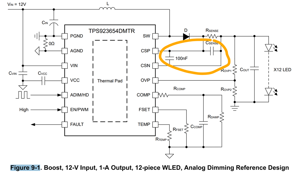
The reason why I ask it because it seems that section 9.2.1.2.5 "Other External Components Selection" may be describing two different capacitors, with two different functions while on the Figure 9-1 both capacitors are in parallel configuration. Why use two capacitors? Is it to reduce ESR? In any case it is a bit confusing. Are two capacitors really required? Please clarify.

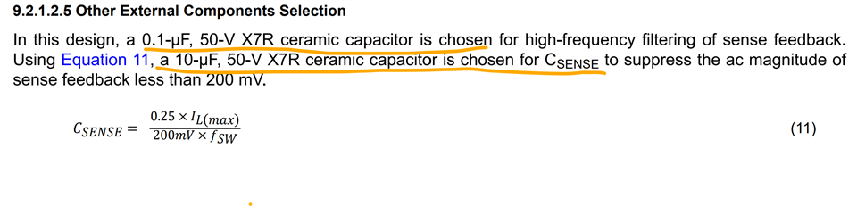
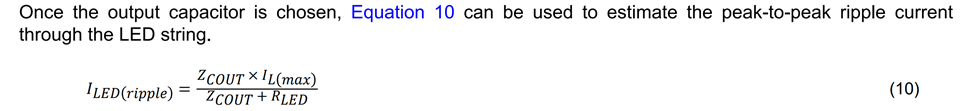
2. In the equation (8) ILED(ripple) is used but then in equation (10) it is calculated. Likely it is a mistake. Maybe in equation (8) ILED(max) should be used instead?
ILED(max) does not appear to be used at all while probably it should be.

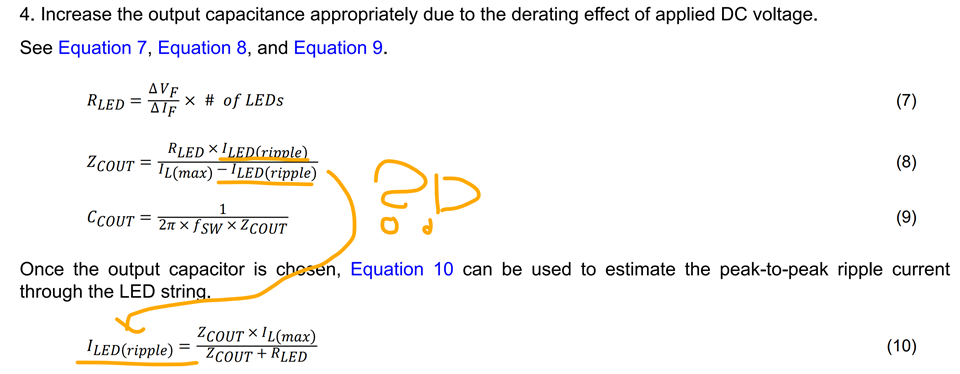
Maybe the answer to the above question is in this sentence: "KIND is a coefficient that represents the amount of inductor ripple current relative to the maximum LED current".
OK, but it appears that in order to calculate max inductor ripple current to select the right inductor I need to know this inductor ripple current first.

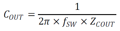
3. Equation (10) in section 9.2.1.2.3 "Output Capacitor Selection" does not contain the value of the chosen capacitor while it probably should. Likely it is a mistake. Please clarify.


4. I am not certain that I correctly understand section 8.3.3 "Undervoltage Lockout". Do I need to connect VCC pin to a resistor divider for it to work and select resistors such that VCC is above 3.2 V(typ)? But the same time VCC pin seems to be the output of the internal LDO 5.15 V(typ).

5. How do I practically calculate Rovp1 and Rovp2 to implement OVP? Let's say I want to make sure that no matter what voltage in the provided example does not go above 40V, even if LEDs get disconnected. Do I correctly assume that Rovp1 and Rovp2 have to be selected such as at 40V output OVP is 1.1 V. "Detailed Design Procedure" (section 9.2.1.2) does not explain that. E.g. how to ensure that the device does not start until Vin > 10V?

6. All I need is just a simple 'analog' dimming but I also need to be able to turn LEDs off completely. Is it enough for that to simply stop PWM at ADIM pin or need to pull EN pin down as well?

7. TPS923653 is said to be working from Vin > 4.5 V but internal LDO provides 5.15 V(typ). I just want to double check that Vin = 5V is OK.

  • Hi Tomasz,

    Sorry. I am currently out of office. I will reply to you tomorrow when I am back to office. Thanks for your understanding.

    Best Regards,
    Steven

  • Hi Tomasz,

    Sorry for the late response. Please refer to below answers to your questions. 

    1. This diagram is correct. As is mentioned in the datasheet, the 100nF capacitor is used for high-frequency filtering of sense feedback. The C_SENSE is a ceramic capacitor with relatively large capacitance to suppress the ac magnitude of sense feedback less than 200 mV (If this large capacitor is missing, you will get a zero sense signal when the internal switching FET turns off and no current flows through the current sense resistor).
    2. In equation (8), the I_LED(ripple) is the LED ripple set by your system spec requirements. You follow this requirement to design the C_OUT theoretically with Equation (8). After you choose your real C_OUT value, you can then estimate the I_LED(ripple) that you will get with this real C_OUT value by using Equation (10). For I_LED(max), yes and there should be one equation. Thanks for pointing out this to us. 
      1. For boost topology, you can calculate I_L(max) with I_L(max) = V_OUT * I_LED(max) / efficiency / V_IN.

      2. For buck-boost topology, you can calculate I_L(max) with I_L(max) = V_OUT * I_LED(max) / efficiency / V_IN + I_LED(max).

      3. When you design the components at the first time, you can estimate a value for the efficiency (like 85%) and use that for calculation. You can later adjust the components based on your test results.
      4. You can take a look at this E2E thread for reference.
      5. There is a mistake in the datasheet sentence "KIND is a coefficient that represents the amount of inductor ripple current relative to the maximum LED current". It should be correct as "KIND is a coefficient that represents the amount of inductor ripple current relative to the maximum inductor current"
    3. You Can calculate C_OUT with this equation.
    4. Please just think about VIN and VCC as the input / output of an LDO. When VIN continuously drops to a value where the LDO cannot maintain its nominal output, the VCC will also continuously drop and finally trigger the UVLO circuitry connected to the VCC pin.
    5. Please refer to this E2E FAQ - [FAQ] How to design the OVP resistor divider for TPS923655 / TPS923654 / TPS923653 / TPS923652? - Power management forum - Power management - TI E2E support forums
    6. It is ok to pull low at ADIM pin to turn off the LED (let the device stop switching), but some internal circuitry will not be shutdown unless you disable the device by using EN/PWM pin. You can refer to these two parameters in Section 7.5 Electrical Characteristics from the datasheet.
    7. The device can work with Vin > 4.5V. Vin = 5V is OK.

    Best Regards,

    Steven

  • Hi Steven,

    Thank you for your detailed response.
    I was more wondering if the 100nF capacitor could be omitted, but I guess it should be there.

    Kind regards,

    Tomasz

  • Hi Tomasz,

    You are welcome.

    Normally I would recommend customer place that 100nF capacitor between CSN and CSP pin.

    Best Regards,
    Steven