This thread has been locked.

If you have a related question, please click the "Ask a related question" button in the top right corner. The newly created question will be automatically linked to this question.

TPSI3050: TPSI3050-each node measuring

Part Number: TPSI3050
Other Parts Discussed in Thread: TPSI3052,

Tool/software:

Hello team,

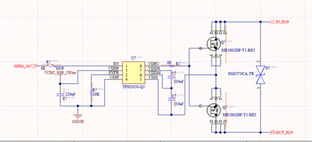
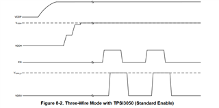
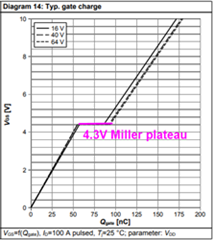
I have some doubt w.r.t the measurement of each node (EN, VDDP, VDDH, VDRV) of TPSI3050. Also, I would like to take measurements and plot a graph as mentioned in your datasheet (Refer below attached image)

FYI, we have 4 channel DSO and I have measured the primary side voltage EN w.r.t GND.

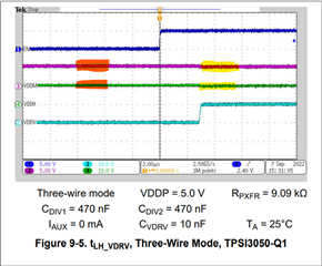
But how to measure the secondary side voltage VDRV and VDDH ?

Looking for your response.

  • Hello Prema Perumal,

    Thank for reaching out to our team on E2E.

    Ideally to make this meaurement, you could use one differental probe on channel 1 to measure EN wrt CGND. Using the other standard probes, you would measure VDDH and VDRV wrt VSS on channels 2 & 3.

    Alternatively, using 2 channels, measure CGND and EN wrt VSS and use the math function to display EN - CGND. Then using channels 3 & 4 measure VDDH and VDRV wrt VSS.

    Regards,

    Jack Hemmesmeier

  • thanks for your reply jack,

    i have some query in this chip,

    1) what is the Vdroop ?is there any issue if the vdroop is above 0.5V?

    2)we are using back to back MOSFETs in a bidirectinal Configguration.how do we calculate the total charge(Qg) of the MOSFETs?

  • Prema Perumal,

    Vroop is how much the voltage VDDH will be lowered by when the load is switched on. Lower VDDH will translate to lower VDRV, resulting in a higher Rdson for the MOSFETS. If VDDH and VDDM fall too low, it will trip UVLO, which is defined in the datasheet as VVDDH_UV_F @ 6.9V and VVDDP_UV_F @ 2.75V for the TPSI3050. 

    The total charge will be twice the value of the gate charge on a single MOSFET. 

    Regards,

    Jack Hemmesmeier

  • Thanks for your reply jack,

    We are using a bidirectional back to back MOSFET(IPTC011N08NM5) with a gate charge of 446nC.Below is the attached graph showing the measurements at all nodes, but the turn-on time is high. How can we reduce this time?

    The calculated value for Cdiv1 and Cdiv2 are 2uf each.Because of that we have 5ms delay from EN to VDRV high, In 2 wire mode. We have to bring down the delay to uS by using low value cdiv , what will be the impact on VDDH droop or in MOSFET operating mode Is it advisable to select tpsi3052 with 15v gate drive voltage with low cdiv capacitors.

    we are tested our design below attached graph also,

    1)yellow -EN

    2)pink-VDRV

    3)blue-VDDH


  • Hello prema,

    Thanks for reaching out to our team on E2E. At a high level, there’s two ways to improve tSTART:

    1. Increase power transfer
      1. Since you already have RPXFR = 20 kohm, the other option is to go from 2-wire mode --> 3-wire mode.

    2. Reduce capacitance loading
      1. Reduce CDIVx
        1. Since reducing CDIVx increases droop, let’s check the MOSFET’s VGS vs. Qg graph.


          Miller plateau looks to be 4.3V where MOSFET RDSON is high, since our UVLO will always be well above that we should be safe. Let’s check our device UVLO to see the what the maximum droop we can get with is.


          Looks like we can target 1.4 V droop on VDDH. If we target higher Vdroop, we risk turning on at the minimum VDDH rising threshold and immediately hitting the falling UVLO, which would shut off VDRV until we charge up to the VDDH rising threshold again. Let’s check 1.4 V droop in our calculator now to see what CDIVx values to use. We can also calculate this using the Q=CV equation.


          We recommend using CDIV1 and CDIV2 values as close as possible to 637.3 nF in order to minimize tSTART and to guarantee the droop is always above UVLO. The calculator tool shows tSTART = 448 µs here but since it’s extremely conservative, the actual start time should be much faster. 

        2. Select MOSFET with lower total gate charge (Qg)
          1. We can further reduce tSTART by using a MOSFET with lower Qg. But I am guessing this is challenging as the application requires high power.

      Best regards,
      Tilden Chen


      Solid State Relays | Applications Engineer

    1. Thanks for your detailed reply Tilden,

      1.How do i measure VDDHdroop  voltage?

      2.Can you explain where i need to clip the voltage probe?

    2. Prema Perumal,

      On channel 1, measure VDDH wrt VSSS. (Probe on pin 7, ground on pin 5) 

      On channel 2, measure VDRV wrt VSSS, and trigger on this channel. (Probe on pin 7, ground on pin 5)

      VDDH droop will be the difference in voltage when VDDH is the lowest and the steady state voltage. 

      Here in the application curve below, I have highlighted the steady state value in orange, and the point at which VDDH is the lowest after VDRV has risen. 


      Regards,

      Jack Hemmersmeier 

    3. Hello Jack,

      Thanks for your valuable feedback!!

      I have some additional open points listed below:

      1. According to the TI calculator, C49(Cdiv1) and C50(Cdiv2) are calculated to be around 2µF. However, this capacitance results in a delay when turning on the MOSFET. Therefore, I am considering using a 1µF capacitor. If I select a 1µF capacitor, what will be the impact on the circuit (specifically, the Vdroop, which is 0.8V)?and what is the tRecover time?

      2. For the TPSI3050-Q1, if I select the 3-wire mode combination, what will be the VDDP current consumption when C49(Cdiv1) and C50(Cdiv2) are fully charged? Will it continuously consume current?

      3. 3Wire mode Whenever i set EN_pin -High or Low VDDP pin is consuming current 36mA, Usually it will happen like this or not?

      Thanks,

      Prema

    4. Premal Perumal,

      1: Changing Cdiv1 & Cdiv2 to 1uf will result in a droop of ~0.9V and tRecover will be at 53.8 us according to the calculator. 

      The device work by storing energy in Cdiv1 and Cdiv2 as energy is transferred form the primary side to the secondary side of the device. When the devices switches on the load, it connects Cdiv1 and Cdiv2 the gate capacitor of the FET. Charge from the capacitors moves to the gate of the FET. According to the equation Q=CV, the voltage must fall considering that the charge has been reduced; this reduction in voltage is Vdroop. Charge is replenished slowly across the isolation barrier. The time taken to fully replenish the capacitors is tRecover.

      2 & 3. The TSPI3050 consumes a content power from the VDDP pin, regardless of whether the EN pin is high or low. The current you are observing is a typical for the device when Rpxfr = 20k and the device is running off of 5V. According to the datasheet, 37mA is the typical value for current consumption. 

      Regards,

      Jack Hemmersmeier