Other Parts Discussed in Thread: UCC21530, UCC21520, UCC28951, UCC28950, UCC27714EVM-551
Tool/software:
Hello Mike,
Hope you doing good and are back from vacation.
Couple of problems to discuss. Below are new updates .
1. I migrated to using isolated gate drivers on primary side as I have switched to SiC FETs since I will be moving to higher voltages. Additionally , I'm using isolated gate driver on output side also ( though reinforced is not required ), but for proto I'm using it. UCC21530 PRIMARY side, UCC21520 SECONDARY synchronous side as per my board functionality. Propagation delays should match / cancel out at input and output side.
2. Additionally I'm not using Shim inductor as of now, as Excel values suggest not to.
3. Rsum : 127k, controller is in CCM Mode always. Current sense : 10R, current sense reset resistor: 1.2K ohm.
4. Output windings in parallel, vout regulated to 13.1V.
Q1. I had trouble going higher voltages due to loop compensation based on values Suggested by excel sheet, so I put a small capacitor ( 1n ) across EA- bottom divider resistor and ground, which helped moved to higher voltages. Maybe layout noise issues or something need to figure out ? Is this ok to add ?
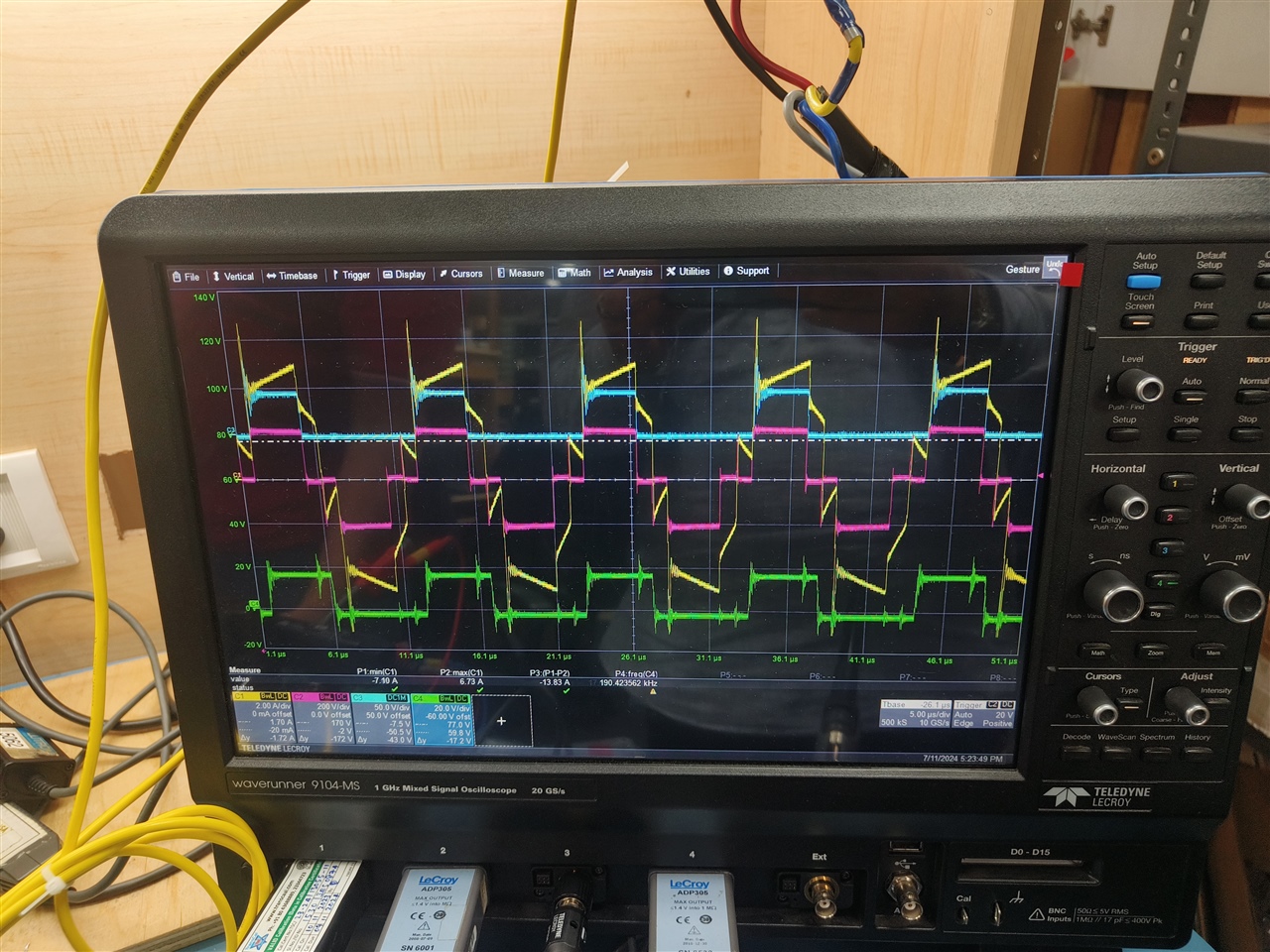
Q2. When going higher voltage or when it's tarts to regulate around 140V and higher ... Transformer current starts to shift negative during the positive edge. For low voltages low load currents it all looks ok, transformer current remains symmetrical across zero crossings. Is it something to do with compensation or duty cycle ? Or is it something different? Please advise.
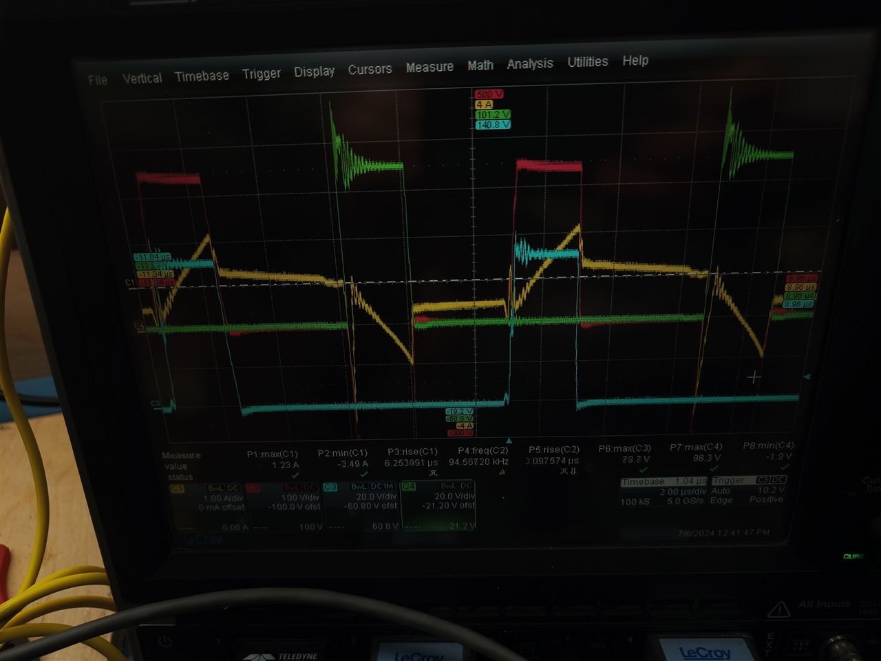
Yellow : transformer primary current
Blue and green : secondary side FETs
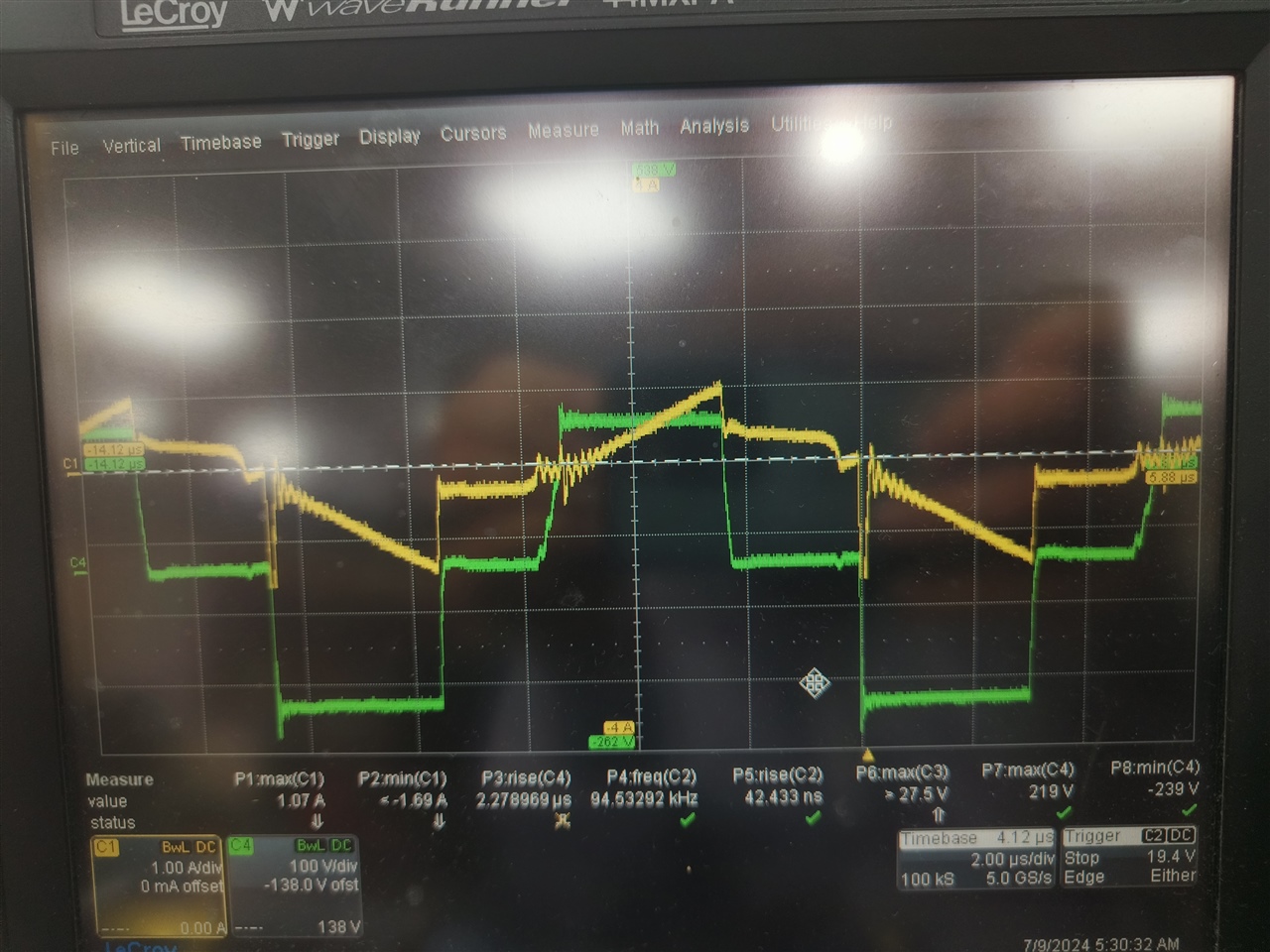
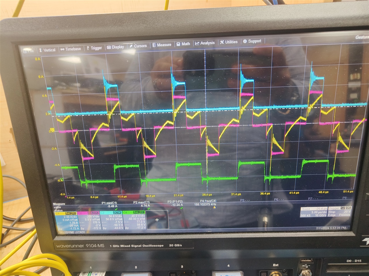
Yellow : transformer primary current
Green : transformer primary voltage
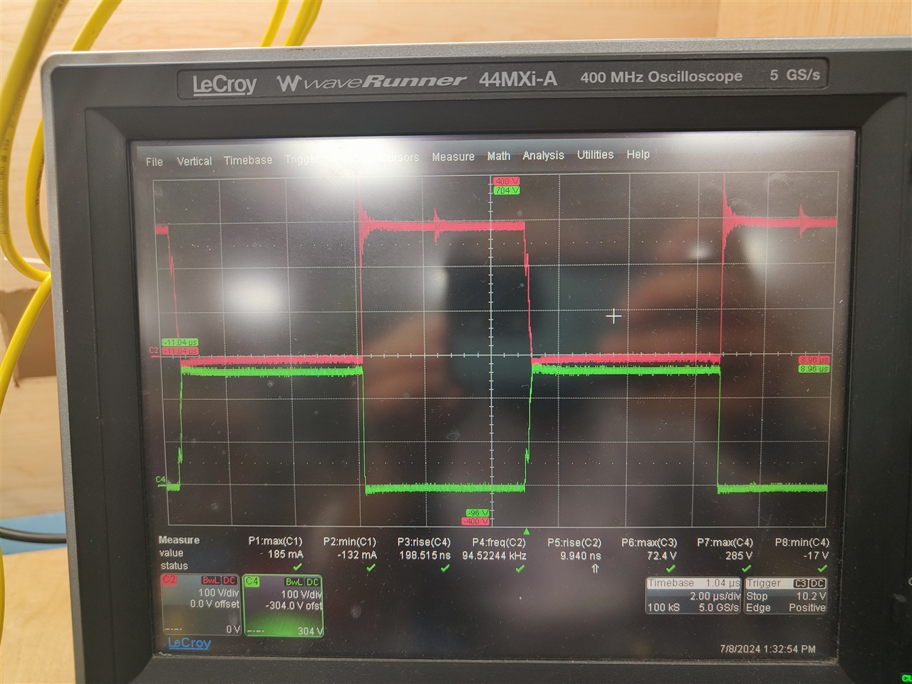
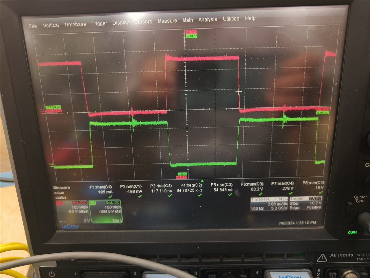
Q3: continuing above problem, Additionally transformer voltage drops momentarily and rises again during higher voltages / higher currents as seen in below image. 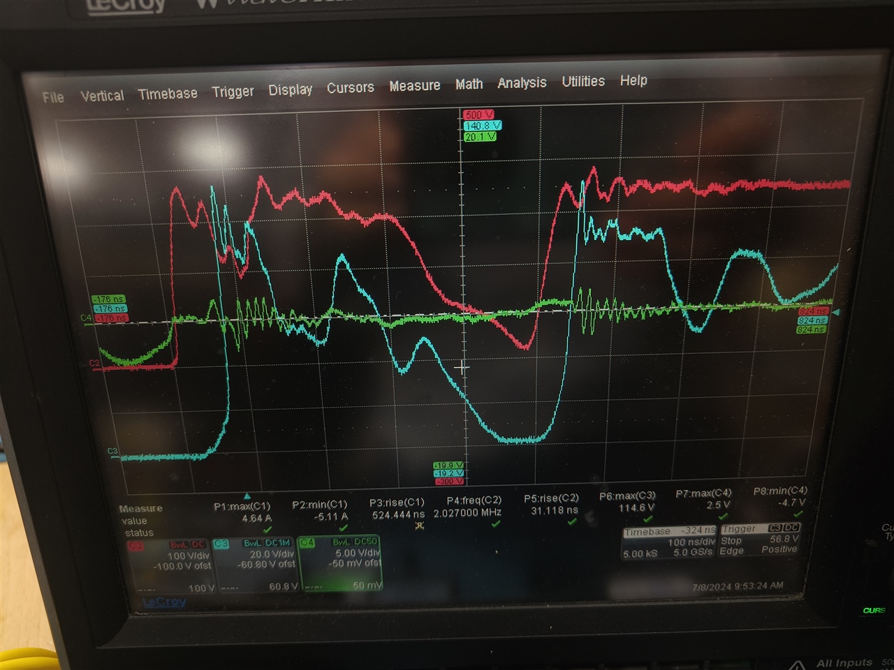
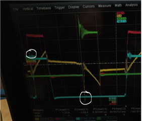
Red : transformer primary
Blue : one of secondary side FETs drain source
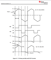
Zoomed out version of above image is below. one of the Synchronous FETs gate in green which turn oFF and then this happens. Is it something to do with reverse recovery of FET diode ? Your thoughts please.
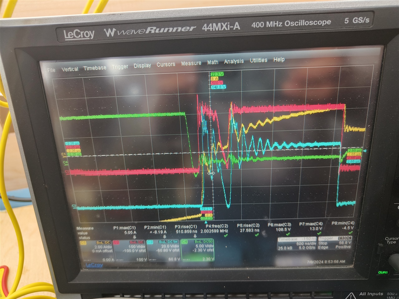
Q4. Also I noticed with introduction to gate drivers , below are gate waveforms primary side switches.
FYI, DELAB : 30K, DELCD: 30k, DELEF:15k
A& B waveforms:
C & D waveforms :
Rise time is different, worst in case of A & B, which I have observed causes a delay in transformer primary voltage postive side, the rise of transformer primary voltage looks slanting and doesn't look sharp which in turn effects secondary side FET also.