This thread has been locked.

If you have a related question, please click the "Ask a related question" button in the top right corner. The newly created question will be automatically linked to this question.

BQ25756: Transient Creating Higher Ripple Current in Control Loop

Part Number: BQ25756

Tool/software:

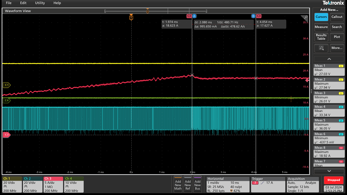
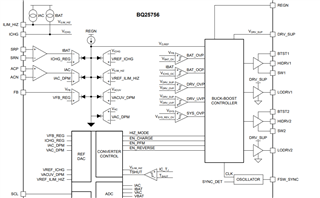
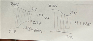
Hello, I am testing with the BQ25756E evaluation board at the moment and have only changed the Richg resistor to 2.44k to produce a charge current close to 17A, all other components are stock. I checked beforehand and the stock mosfets and inductor seem to be able to handle the increased current. My testing scheme consists of the power supply, the charger board, and the battery. My Vchg=29.4V, Ichg=17A, Fsw=250kHz. 
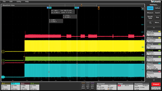
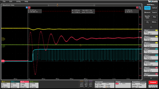
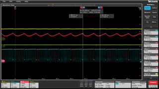
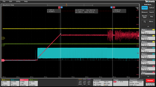
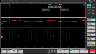
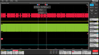
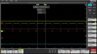
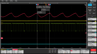
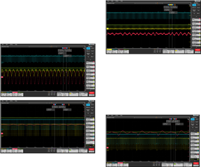
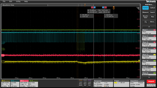
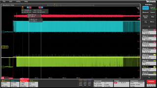
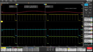
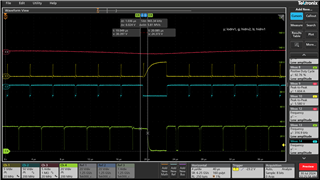
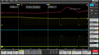
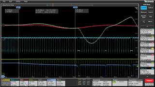
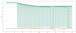
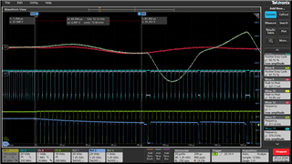
Red: Ichg, Yellow=Vout, Green: LODRV1. Blue: HIDRV1.

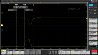
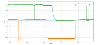
My battery voltage is 27V, so I am expecting a full charge current of 17A at turn on. When I turn on any of the three while the other two are on, in a minority of cases I see a normal turn on where Ichg=17A, Fsw=250kHz, and Iripple=~2A. However, most of the time I am seeing an oscillating turn on where Fsw=~133kHz aka 1/2 of programmed value, and Iripple=~5-7A, which causes my Iout to be ~17.9A at steady state. This oscillating behavior exists for 0-2minutes before eventually it returns to normal Iripple.

What could be causing this, and is there any way to fix this? Any help is appreciated.

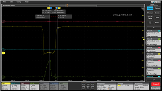
I will include waveforms of the steady state, gate drives, and transients below.
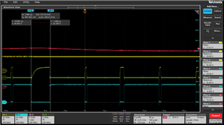
I've noticed that at a normal turn on event, Fsw=~133kHz during the current ramp up, before evening out to ~250kHz when Iout begins to be regulated is this intended? If this is intended, does the charger think it is in ramp up mode still? None of these behaviors occur with Eload testing, only battery load.

  • Hello Michael ,

    Thanks for being patient with this. We are very busy right now and I will get back to you later on this week.

    Best Regards,
    Ethan Galloway

  • Note the 4kHz audible frequency in the ripple current image above. With 10A stock board I am measuring ~14kHz.

    This same "oscillating turn on" behavior happens in a stock board with no modifications charging at 10A as well with Ipkpk=~2App (1.4App w/ normal turn on) and ringing occurs as well, albeit at a higher pitch (frequency). Both normal and oscillating turn on events occur with the stock board. Waveforms for the stock board are shown below. Red: Ichg, Yellow=Vout, Green: HIDRV1. Blue: none.

  • Hello Michael,

    Thanks for the new information. This will be very helpful as I look into this.

    Best Regards,
    Ethan Galloway

  • Hello Ethan, I have more information from testing.
    I am using a supply set at 30V with 25Alimit. It seems like this current disruption is occurring at when my Vin is close to my programmed Vcharge=29.4V. Testing with Eload we are seeing the current disruption in a Vin range of 28V to 30.2V as the charger nears its bucking/boosting transition point.  This causes a ripple of ~0.6Apkpk, which is acceptable to us, but when testing with battery load we are seeing close to 2-3Apkpk, which is not acceptable for our application. Is there any way to reduce this ripple's amplitude and frequency and therefore the audible ringing near the transition point?

  • Hello Ethan, I have more information from testing again.
    We have isolated the problem to us being in the transition region from buck to buck boost since our testing scheme had Vin=30V and Vchg=29.4V.
    We have identified this problem (high output current ripple) as happening only in the transition regions in and out of the buck-boost mode. It happens at any Ichg and Vchg. The waveform shapes vary, but are always present in this region. In other words it happens when buck SW1 is on and boost SW2 begins turning on, but is stuttering. (entering from buck to buck-boost) and vice versa when entering from boost to buck-boost. Are there any steps we can take to resolve this issue?

  • Hello Michael,

    Thanks for being patient with this. I tried doing your test in the lab and I'm not seeing the same issue.

    I am seeing an oscillating turn on where Fsw=~133kHz aka 1/2 of programmed value

    In the buck-boost region, the Fsw= 1/2 of the programmed rate is expected behavior. The buck and boost sides of the circuit activate every other clock cycle.

    Can you answer a few questions about your test to help me with debugging?

    What type of battery is used?

    Does adding a bulk capacitance to the battery change the results? 2000uF or greater should work for the bulk capacitance?

    If you take any more waveform images, can you focus on SW1, SW2, VBAT, and IBAT?

    Are in the constant voltage region or the constant current region?

    Best Regards,
    Ethan Galloway

  • Sure thing.

    1.8S-2P Li-on battery with internal data logging electronics, so I cannot peer inside. 
    2. I will test this and reply again, though in the eval board datasheet, wasn't 2000uF reserved for testing with non-battery loads? What is the thinking behind adding this large capacitance? Note that I am running the eval board above its rated 10A, since I found the stock inductors, mosfets to be able to handle the current, though not sure about caps.
    3. Included images are different oscillations I've captured at different Vchg (29.4V, 31V) and Ichg (5A, 10A, 17A) settings. It doesn't seem to be related to Vchg and Ichg though, just correlates to entering and exiting the buck boost region, which I am accomplishing by varying Vin while charging. (Could speed of variance in Vin and Fsw be correlated? Since I am running at Vin range of 20-36V, I think the design calculator says inductor current reaches quite close to saturation current of the stock inductor) 
    4. I am in constant current region. 

  • Hello Michael,

    Thanks for the new information and thanks for being patient. My reply never got sent.

    1. Got it.

    2. I'm curious to see if the bulk capacitance will reduce the ripple.

    3. Thanks, can you tell me which channel corresponds to which measurement here?

    4. Thanks.

    Best Regards,
    Ethan Galloway

  • Hello I will test the capacitance and get back to you tomorrow. I recently completed testing and am seeing that at higher switching frequencies, there is much less current ripple frequency and amplitude. I have also located where the ripple occurs, it occurs in and around the hysteresis band between the buck and buckboost modes, when I am varying Vin from 35-20V. I also notice that the hysteresis band (where SW1 is ON and SW2 is sputtering, turning on) is close to 0V at Fsw=600kHz, whereas at Fsw=250kHz, it is ~0.1-0.5V. My theory is that the Vout is not stable so as it fluctuates due to the transition of the switching frequencies from SW1 ON to SW1+SW2 ON, we see  a higher current ripple. For example, (Vout-Vbatt)/Rbatt=~0.1Vpp/50mohms=~2App. 

    Vbatt:27.36V, Downwards Vin (35-20V), Ichg=17A, 31Vchg, 600Hz: 32.2-31.1Vosc(3.3App)-31.3Vbuckout-27.6Vboostin. Typical Ioutripple when not rippling: ~0.4App. 

    In the images above, blue is SW1, green is SW2, yellow is Vout, red is Iout. 

  • Hello Ethan, I have completed the capacitor test. I added 1000 at each side of the sense resistor at the output and saw high current ripple ~2App among my entire operating Vin range. The board also got extremely hot, so this would not be suitable for my application. I didn't see any ripple during my test, but board became very hot and steady state ripple was too high.

  • Hello Michael,

    Thanks for doing these tests.

    The board getting hot is expected. The EVM was designed to charge at 10A. I'd recommend to use an external gate drive of 7V or 11V. This will increase the efficiency and should improve the thermal performance.

    I'll get back to you about these tests later on this week.

    Best Regards,
    Ethan Galloway

  • Hi Ethan, I made an error in the previous post, my ripple is ~1App at steady state. Now I am not seeing any ripple, though. Instead, when I transition from the buck to buck boost region I am only rarely seeing a temporary noise increase up to 1.6App. I am also seeing this behavior when I turn on the charger and Vin and Vout places it at the buck boost region threshold. I will attach an image of this below, Red: Iout, Blue: SW1, Green: SW2.

    1. Why should the increased gate drive of 7 or 11V increase the efficiency of the charger?
    2. Also, what was the thinking behind adding the bulk capacitance, was it to reduce output voltage ripple? Was the output voltage ripple higher, causing larger current ripple when the voltage is dropped across the battery, and this disrupted the control loop?
    3. I am seeing the hotspots concentrated around C5 when bucking and C28 when boosting. Why are these specific capacitors getting hot?

    I would like to know this to better understand and diagnose the system in the future. 

  • Hello Michael,

    1. Increasing the gate drive voltage will increase the pull down and pull up gate current and improve the RDS ON of the FETs. A larger pull up and pull current will decrease the switching losses and a lower RDS ON will decrease the conduction losses. At these high power levels, I really recommend using an external gate drive supply.

    When you lay out your own PCB, you can also install more FETs in parallel, this will also help reduce the conduction losses.

    2. I think the battery pack may have had a parasitic component like resistance or inductance that was causing the oscillation. I don't have the battery pack that you have so I can't say for sure.

    3. These capacitors are absorbing a lot current from the buck-boost converter. You can use the BQ25756 design calculator to help calculate the ripple current into the capacitors. C5 and C28 are the closest to the switching FETs and are probably absorbing the most ripple current.

    Another thing to check is to make sure those capacitors aren't reflective. You can put some masking tape, electrical tape, or a sticker over the capacitor to reduce the reflectivity. If you try to measure the temperature of a reflective component, you'll often end up measuring the temperature of the things around the reflective component.

    If you haven't already, I would recommend doing the same thing for the inductors you test with. The default inductor is reflective and a piece of tape will help you take an accurate measurement.

    Best Regards,
    Ethan Galloway

  • Hi Ethan,

    Is there any downside the increasing Vgatedrive for efficiency? I thought that the slower rise time of the switching pulses (I measured rise times of ~76ns vs 100ns for gate drive voltages of 5V and 11V) due to the higher Vgs would reduce efficiency, since switching losses would be increasing. How does the larger pull up/pull down current decrease switching losses?

    And why does switching frequency halve in buck boost mode? Is it for stability/control loop reasons?

  • Hello Michael,

    There should be no downside for increasing the gate drive for efficiency. Keep in mind that with a gate drive voltage of 11V, the FETs still turn-on at 5V.

    For the switching frequency halving, this is intended behavior and is done to make sure there is seamless transition from buck to boost mode.

    Let me know if you have anymore questions.

    Best Regards,
    Ethan Galloway

  • Hello Ethan,

    I had a question about the internal block diagram for the fault signals. I see that there is some kind of diode ORing configuration (see image below) for certain comparators. I assume they would pull REGN current to ground in case a fault triggers and therefore disable the gate drivers. Is this what happens? And if so, why is REGN by default grounded? Also, what is the purpose of the Vo,ref signal? Any help is appreciated, thank you

  • Hello Michael,

    These signals control and modulate the Vo,ref signal. For example, if the charger approaches the battery charge voltage, the VFB comparator starts and begins controlling Vo,ref to put the charger into constant voltage mode.

    These signals are only used during battery charging. That's why they can be powered by REGN because REGN is active while the charger is charging.

    Best Regards,
    Ethan Galloway

  • Hi Ethan, 

    Understood, but then why is REGN as a source grounded at the very bottom? This would make the REGN sink all of its current to ground before and during charging. 

  • Hello Michael,

    To clarify, the diagram shows a current source pulling from REGN to GND. This way the REGN source doesn't collapse.

    Best Regards,
    Ethan Galloway

  • Thanks for the clarification so far Ethan, this has been very helpful for the proejct and we are leaning towards BQ25756 for our usecase. To check my understanding, so each OTA will pull different amounts of current from REGN to ground when their conditions trigger. Then this will change Io,ref which flows through a resistor to develop Vo,ref. Vo,ref's value is something something specific that the controller can recognize and the controller will decide on an action corresponding to the OTA that triggered it?

  • Hello Michael,

    Yes, I believe that is how the charger works. The charger has a lot of different control loops running at the same time that take control of the converter at different times.

    Best Regards,
    Ethan Galloway

  • Hello Ethan,

    I have come back with more testing results. I have located the error down to the entry and exit points of the buck boost mode. I am at IChg: 17A and Fsw: 600kHz, without the 2000uF capacitors, which I found to not affect ripple significantly. When I am barely in buck boost mode (both legs are alternating switching cycles), I am seeing current ripple when it is the buck leg's turn to turn on (aka Vin feeds Vout), it suddenly switches off. And then boost leg instead kicks on and charges the bootstrap cap higher.


    In the image I have attached below, I have overlapped two sets of waveforms taken right after each other. Red, sky blue, and green are Iout, LODRV1, and LODRV2 at the moment buck boost is entered with Vgatedrv1: 11Vext. The other colors are the equivalents with Vgatedrv: 5Vregn. It looks like the bootstrap cap is not being charged fully at 5V, as the top voltage of the signal is falling from 37.3 to 31.3V before the legs drop off, then it comes back on at the next cycle at 32.5V and drops off again at 31.5V. Any idea why this could be happening?

    My theory is that the charger captures the compensation values "for a given set of passives" at startup. I also know that a decreasing Vgs over time means a lower Qg over time and so the charging times of the mosfets change over time. It also means Rdson changes over time, either of which the charger could not be accepting. So when the datasheet mentions calculating compensation values for a given set of passives, which passives are taken into account and could the charge characteristics effect the compensation values the charger generates?

    Thank you for the help,
    Michael
      

  • Hello Michael,

    Thanks for being patient with this. I will get back to you later on this week.

    Best Regards,
    Ethan Galloway

  • Hi Ethan,

    Thank you. I have found this ripple to occur even with completely stock boards near the buck boost mode transition voltages. I should add that the 2000uF output caps probably help a little in reducing current ripple but does not solve the root ripple problem. I am curious if this ripple is due to the controller or board layout, or otherwise. Again, so far my fixes have been to increase switching frequency to 600kHz to avoid inductor saturation, and increase Vgatedrv: 11V, which I have not seen ripple in yet.


    I've also captured these two waveforms of the buck and boost top and bottom legs (yellow is top and green are bottom legs, left image is buck, right is boost). These seem quite degenerated to me, are they can issue? I am seeing them in the stock board as well, in all modes.


    And here is an image of different rippling waveform captured this time.


    Notably I am noticing the ripple occurring when the controller is in buck boost mode and turning high side buck fet HIGH to start a new buck cycle, but it is interrupted midway and the high side boost fet is suddenly pulled high to charge the inductor. See images below.
    In left image) Yellow: Lodrv1, Blue: hidrv1, Green:Hidrv2, Red: Iout
    In right image) Yellow: Hidrv1, Blue: none, Green: Lodrv1, Red: Iout


    Boost Side hidrv(yellow) and lowdrv(green) signals during this dropoff.

    In the image below you can see two types of this dropoff, one where buck hi side fet turns LOW while boost side fet is plateauing, then becomes LOW. And one where buck high side FET is ON and boost high side FET is plateauing, then the buck turns LOW and boost turns HIGH. It's almost as the transition into the buck boost mode destabilizes the controller and makes it begin shutting off the buck then boost side high side FETs at 25kHz intervals (frequency of ripple)


    This behavior only happens at the transition from buck to buck modes at Fsw: 600kHz. Near this mode the controller begins adding 300kHz cycles in between its 600kHz buck cycles as we approach buck boost mode. This happens for both Vgatedrv: 11V and 5V, but with 11V, the voltage range it spends phasing in and out the 300kHz cycles is much lower. Also at Vgatedrv:5V, boost cycles begin phasing in and out while buck cycles are on, forcing buck cycles to change between 300kHz and 600kHz abruptly. Maybe the controller doesn't respond well to that as it needs to jump the duty cycle of the boost side from 0% to 97% and the buck side ~10-20% as boost kicks on. 

  • Hi Ethan,

    Thank you. I have found this ripple to occur even with completely stock boards near the buck boost mode transition voltages. I should add that the 2000uF output caps probably help a little in reducing current ripple but does not solve the root ripple problem. I am curious if this ripple is due to the controller or board layout, or otherwise. Again, so far my fixes have been to increase switching frequency to 600kHz to avoid inductor saturation, and increase Vgatedrv: 11V, which I have not seen ripple in yet. 


    I've also captured these two waveforms of the buck and boost top and bottom legs (yellow is top and green are bottom legs, left image is buck, right is boost). These seem quite degenerated to me, are they can issue? I am seeing them in the stock board as well, in all modes.


    And here is an image of different rippling waveform captured this time.


    Notably I am noticing the ripple occurring when the controller is in buck boost mode and turning high side buck fet HIGH to start a new buck cycle, but it is interrupted midway and the high side boost fet is suddenly pulled high to charge the inductor. See images below. 
    In left image) Yellow: Lodrv1, Blue: hidrv1, Green:Hidrv2, Red: Iout
    In right image) Yellow: Hidrv1, Blue: none, Green: Lodrv1, Red: Iout


    Boost Side hidrv(yellow) and lowdrv(green) signals during this dropoff.

    In the image below you can see two types of this dropoff, one where buck hi side fet turns LOW while boost side fet is plateauing, then becomes LOW. And one where buck high side FET is ON and boost high side FET is plateauing, then the buck turns LOW and boost turns HIGH. It's almost as the transition into the buck boost mode destabilizes the controller and makes it begin shutting off the buck then boost side high side FETs at 25kHz intervals (frequency of ripple). This dropoff behavior happens with an external gate drive of up to 5.3V and stops at 5.4-5.5V.


    This behavior only happens at the transition from buck to buck modes at Fsw: 600kHz. Near this mode the controller begins adding 300kHz cycles in between its 600kHz buck cycles as we approach buck boost mode. This happens for both Vgatedrv: 11V and 5V, but with 11V, the voltage range it spends phasing in and out the 300kHz cycles is much lower. Also at Vgatedrv:5V, boost cycles begin phasing in and out while buck cycles are on, forcing buck cycles to change between 300kHz and 600kHz abruptly. Maybe the controller doesn't respond well to that as it needs to jump the duty cycle of the boost side from 0% to 97% and the buck side ~10-20% as boost kicks on. 

    Steps to Recreate Issue: 
    1. Connect power supply to stock eval board. Connect stock eval board to battery, not Eload.
    2. Install clamp current probe on output + wire. Install 2 voltage probes on HIDRV1 and 2.
    3. Start charging battery with stock configuration and at Vin: 33V. 
    4. Lower Vin until buck boost mode occurs. Current ripple should be seen. Sometimes it does not occur for a few tries (this indicates instability at buck boost transition to me).

  • Hello Michael,

    Thanks for giving us the exact steps to recreate this issue. I'll look into this and get back to next week. Thanks for being patient with this, I've been swamped the past two weeks.

    By the way, for operating at 600kHz, you may want to move to a switching FET with less input and output capacitance. I think a FET like the SiR188LDP or the AON6380 will help reduce the switching losses here.

    Best Regards,
    Ethan Galloway

  • No problem, Ethan I am interested to see what you find. I am charging a 8S-2P Li-On battery by the way.

    Ok after thinking on it some more, here is what I think, let me know your thoughts. 

    Proposal:

    Extreme heat (0-80C in 3 seconds at 17A) at input and output caps decreases capacitance after startup and affects frequency response of converter, which is using captured compensation values at startup to operate. The values are generated from “a given set of passives” at startup. Could be resolved with layout adjustments to prevent sudden component heating. 

    Evidence for this proposal:

    • Evidence: For Vgatedrv: 5V, charge currents above 15A produce current ripple
    • Reasoning: So higher charge currents mean suddenly thermal stress on mosfets and caps, which change their ratings. 
    • Evidence: For Vgatedrv: 11V, no charge currents produce ripple. Bootstrap capacitor is no longer being more discharged then charged.
    • Reasoning: Vgs (and therefore Qg and Rdson) are changing after compensation values are captured. 

    Two factors that are shown to effect ripple: charge current and Vgatedrv supply voltage. (and Fsw which is maxed out, so not relevant here)

    Related Factors

    • Why does ripple occur at buck to buck boost mode transitions and not boost to buck boost?
    • Buck and Boost positive duty cycles rise and fall ~80-90% at buck boost transition modes. Large changes in duty cycle could effect stability. So changing Vgatedrv or Ichg can effect stability somehow.

      Key Question: What kind of passives does the compensation take into account when it toggles the SW node at startup? Do FET parameters effect it in anyway?


      Updated Test Plan:
      1. Connect power supply to stock eval board. Connect stock eval board to Li-On battery, not Eload.
      2. Install clamp current probe on output + wire. Install 2 voltage probes on HIDRV1 and 2.
      3. Start charging battery with stock configuration and at Vin: 33V. 
      4. Lower Vin until buck to buck boost mode transition occurs. Current ripple should be seen. Sometimes it does not occur for a few tries.
      5. Change converter to be 17A of charge current and 600kHz. Repeat step 4 and observe for ripple. Current ripple should be seen. 
      6. Use 11V external gate drive supplyRepeat step 4 and observe for ripple. No ripple should be seen. 

  • Hello Michael,

    Thanks for being patient with this and thanks for the test procedures.

    It makes sense that an 11V gate drive removes the ripple. The FETs are being pushed to the absolute limits at 17A.

    What kind of passives does the compensation take into account when it toggles the SW node at startup? Do FET parameters effect it in anyway?

    I'll need to look this information up.

    Best Regards,
    Ethan Galloway

  • 1. Could you please elaborate on what you mean by absolute limits? Which parameters of the FET, bootstrap cap, or the gate driver could potentially be violated?

    2. This is a comparison of a good boost leg (blue) vs a bad boost leg (green) gate voltage @ the buck to buck boost transition.
    Bootstrap cap on-time voltage (via top voltage) is intended to be taper off and stabilize via the programmed controller duty cycle, as shown in blue waveform. But in green, it does not and continues to drop the top voltage below until it hits a value that is below the mosfet Vgsth. Then controller drops off both boost and buck legs (buck not shown here), giving the bootstrap cap enough time to charge above Vgsth again. 

    This is what i believe to be happening, I know MOSFET Vgsth is being violated, but im not sure:
    1. how the controller could shut down both HS FETs once Vgsth is violated
    2. why the top voltage continues to decrease and not stabilize in the bad boost waveform


    Data Captured

    Waveforms captured: Vbatt: 26.7V, Vout: ~27.1V, Vgsth:2.5V, Vgson=Vout+Vgsth=29.6V.

    Measured before bottom voltage rises (85us)

    • Bad Boost: T=3.551us, Ton=3.38us, D=0.952us

    Measured at 3 cycles before dropoff occurs (bottom voltage at almost max value, 128us):

    • Good Boost: T=3.554us, Ton=3.391us, D=0.954us
    • Bad Boost: T=3.544us, Ton=3.36us, D=0.948us //D has decreased below 0.95!

      Left: Bad Boost // Right: Good Boost

    So maybe in bad version, boost leg reaches internal controller limit for boost duty cycle (maybe D=0.95) right before shutoff.
    We know for certain Vgs < Vgsth at bad boost waveform )comparing Vgson and Vdiffs in image) right before shutoff. So maybe Vgs violation is what causes turn off.

  • Hello Michael,

    1. I should have clarified here "Absolute limits" here. I meant this to mean that the FET is being stressed far more than usual here. With 17A charger current and 5V gate drive, these FETs and the IC would be really hot. Have you used a thermal camera to measure the temperature of the FETs with a 5V gate drive compared to an 11V gate drive?

    Also, keep in mind, that higher temperatures increase the leakage current of most devices.

    2. The charger automatically turns OFF the high side FET to refresh the boot strap capacitor. This typically happens at 3.1V and this information is available in the datasheet.

    For why the voltage is continuing to decrease, I think the high temperatures have increased the gate leakage current of the FETs or the IC. The capacitor voltage falls faster than normal causing a BTST refresh.

    Best Regards,
    Ethan Galloway

  • Hi Ethan,

    1. I am not seeing high temperatures on the FET on the top side, but I am on the bottom side where the exposed pad is. About 80C rising (Vgatedrv: 11V) and 109C rising (Vgatedrv: 5V) after 1 min. So it is getting quite hot.

    2. Ok I rechecked and found the 3.1V value in the datasheet, thank you sir. This is a critical piece of information.

    3. Ok and so connecting the BTST refresh with the current ripple: When refresh happens, Buck and Boost both drop off so that caps can be charged again. This causes output current to decrease (this is the current ripple valley), causing controller to react and increase duty cycle to raise current. Then both legs kick back on at the next cycle and current suddenly increases on top of the increase generated by the control loop (this is the current ripple peak). So then controller will try to lower its duty cycle to lower current. But before it can do that a second dropoff of the legs occur and the cycle repeats. Does this sound about right?


    4. When a BTST refresh occurs, it looks like the image below (Green: Boost HS GTDRV, Orange: Buck HS GTDRV). Is there any reason why the buck gate signal seems to be pulled down to ground and the boost side seems like it is discharged capacitatively?

    5. Is there any reason we are seeing this bottom voltage rise? It corresponds to when the boost leg continues dropping past its stabilization voltage. I thought this was hinting towards a max duty cycle violation issue as perhaps the controller can't pull down the signal fast enough before the next cycle starts, but with what you said it may be the leakage current. 


    6. Reason to be skeptical of leakage current: this behavior doesn't happen on the buck leg at boost to buck boost region. This only happens in buck to buck boost transition modes. So this implies it is tied to the transition aka the controller logic or the 0-95%) duty cycle jump as boost cycle kicks in. It also implies this is a boost side gate driver/bootstrap cap only problem. Buck and boost legs never experience this in their normal modes even as they see high temps that increase leakage current throughout operation.

  • Hello Michael,

    Thanks for these measurements.

    1. Thanks for taking these measurements. 109 C after 1 min is extremely hot. I don't think you should be running the FETs like this. Keep in mind that the current and rated power dissipation of FETs decreases as these FETs get hotter. Also, if you have trouble getting good readings, stick some masking tape or electrical tape over the component.

    2. Your welcome

    3. I'll need to look into this.

    4. This may be the result of the switching node falling slowly. Keep in mind, that the HIDRV signals are referenced to the switching nodes and not GND.

    5. I'm can't tell just from this image alone. What are your red and orange signals?

    6. I don't think we can support the BQ25756 with a 17A charge current, 600KHz switching frequency, and 5V gate drive. The power loss from the FETs is extremely high in this configuration and there could be any number of factors that could be messing up here. The FETs are derating at this high temperature. The capacitors will derate if they get hot as well.

    Let me know if you have any more questions about this and let me know if using an 11V gate drive works for your application.

    Best Regards,
    Ethan Galloway

  • Hello Ethan,

    I have discovered the root cause of the problem. Thank you for your help, your insights helped me resolve the issue.