This thread has been locked.

If you have a related question, please click the "Ask a related question" button in the top right corner. The newly created question will be automatically linked to this question.

Problems with Power supplies designed with Switcher Pro (TPS40054 & TPS54620)

Other Parts Discussed in Thread: TPS54620, TPS40054, TPS40055

I have used the Switcher Pro program to design 5 power supplies. A 12V 6A based on the TPS40054 and 5V, 3V3, 1V9, 1V2 based on the TPS54620.

The TPS54620's are fed by the 12V supply, so lets start with the 12V supply first (Switcher Pro report:4721.12V.pdf SCH: 7462.supplies.pdf PCB:4405.supplies_pcb(top+mid1).pdf 0844.supplies_pcb(mid2+mid3).pdf 1273.supplies_pcb(bottom).pdf).

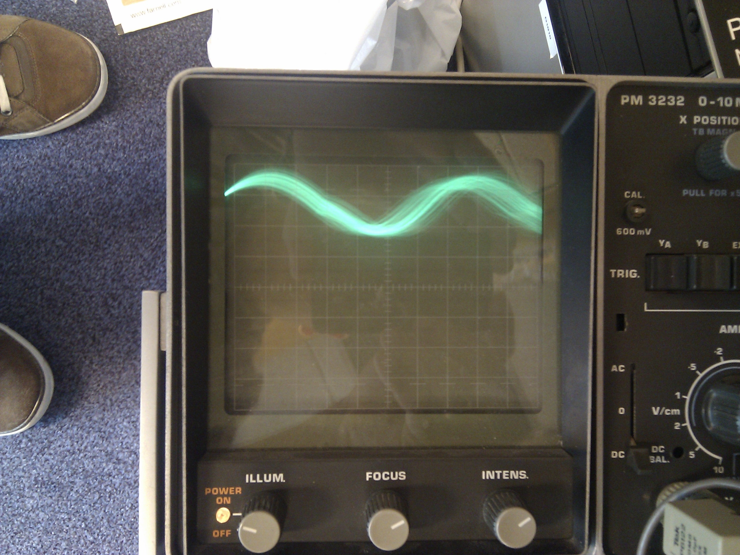
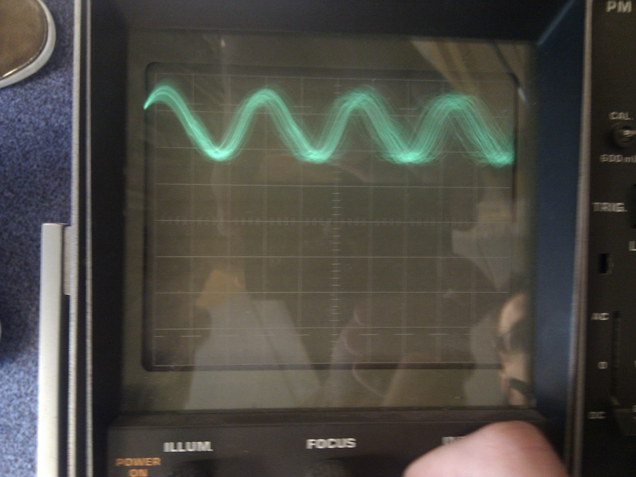
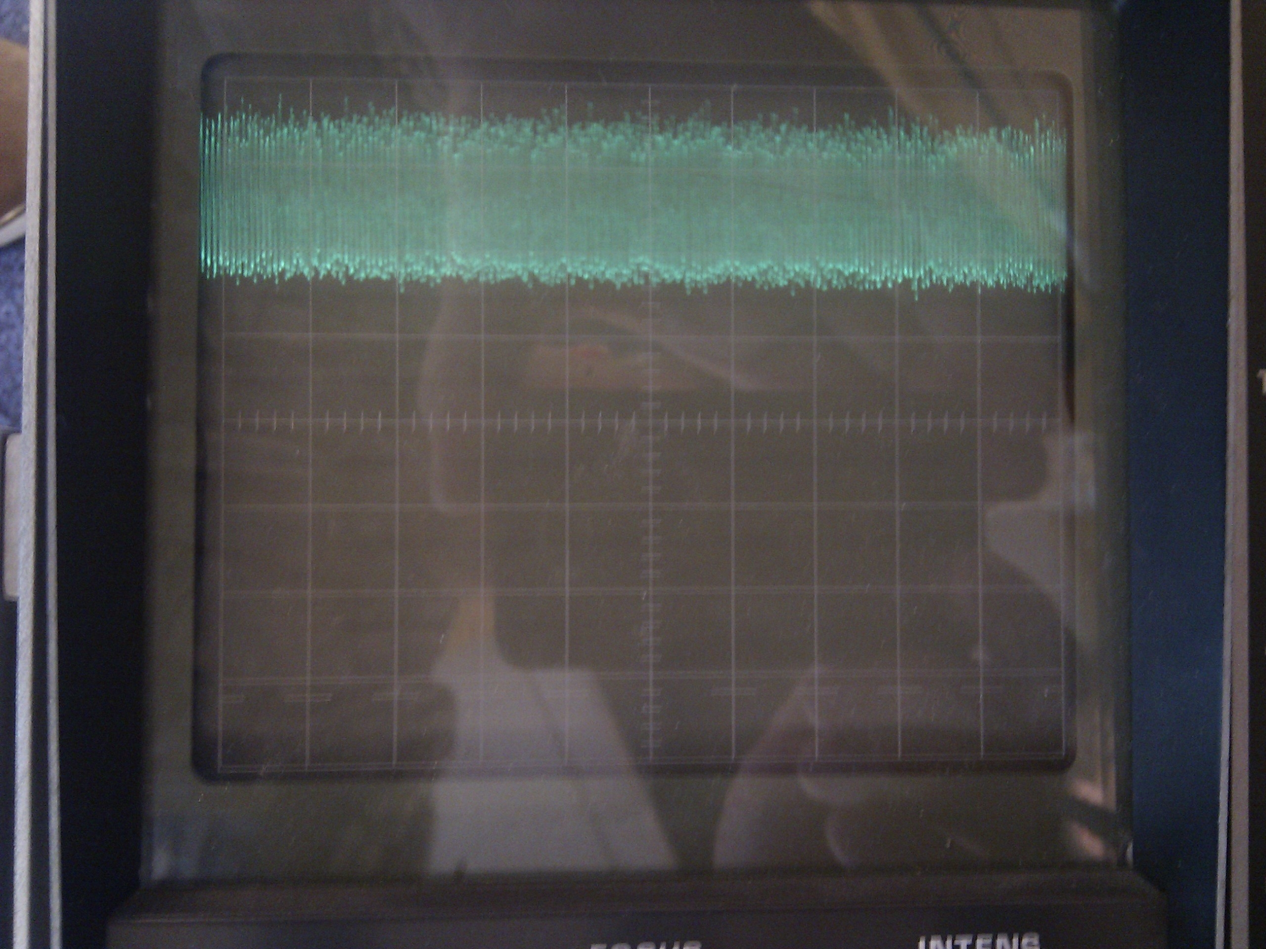
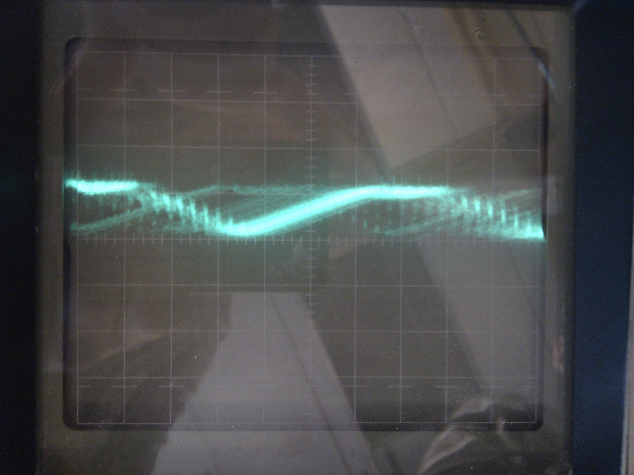
The 12V supply was designed with a f_sw of 200khz, but as I want to synchronize the supplies I use an external oscillator to provide 200khz and changed Rt to 330k to get a free running freq of 161kHz so that 200kHz falls in the 20-30% higher range as stated as necessary in the datasheet. C_ss has been increased to 68nF to ramp somewhat slower.

Observations so far on 12V supply:

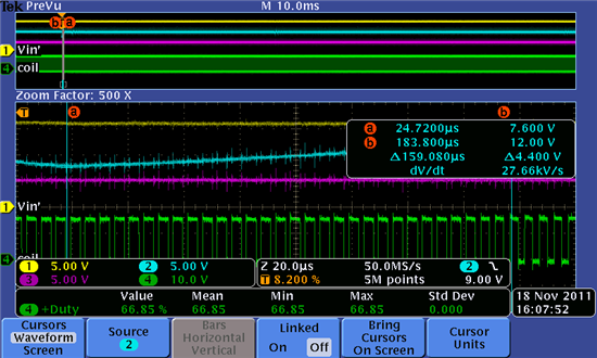
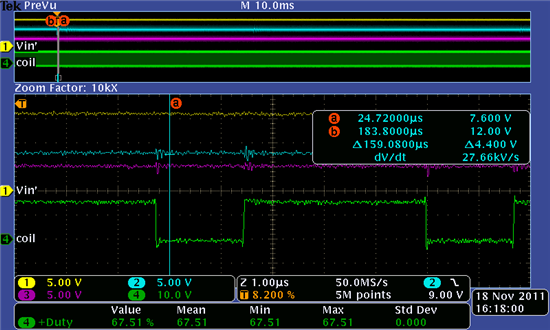
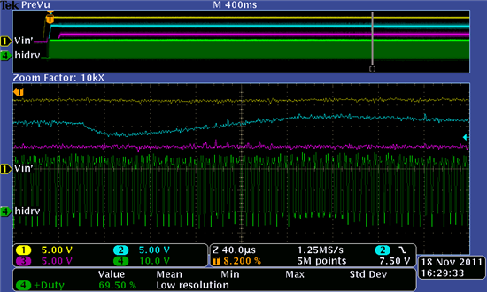
- The frequency of the sync signal was initially to low (~170khz), the device however starts providing 12V if the input voltage is just above the UVLO of 14.4V. If I increase the input voltage the output voltage drops to 6-8V. If I add load (1.5A) the voltage dips to 11.6V at the output of the coil.

- If I increase the sync frequency to 200 kHz I have to decrease the value of Rkff, or the device does not seem to start. I also have to connect additional load (the circuit itself provides very little load until the 12V is within limits), the voltage on the output is only 9.7V (Vin=16V) to 9.9V (Vin=24V). 


Efficiency is important in this application as the board is battery powered (18-36V). Therefore I have (hopefully correct) chosen a low switching frequency and large coil.

Any pointers on where to start debugging?

  • What type of problems are you having with the TPS54620 circuits?

  • Testing things with the 54620s is a bit difficult due to the problems with the 12V input, but one thing is that although the datasheet states that the rising threshold on the ENABLE pin is 1.26V max, the supply does not start with 1.32V (measured) applied to it. If i force it to 3.3V  3 out of 4 supplies start and assert their power_good signal. The 1V2 supply however does not assert power_good. 

  • Let me state my questions about the 40054 a bit more explicit:

    • I used the PSMN014-60 5658.PSMN014-60LS.pdf from NXP as top and bottom mosfets. Are these maybe not so well matched with the TPS40054?
    • I changed the value of the coil (in SwitcherPro) to be bigger to improve efficiency of the circuit. Are there drawbacks to doing this?
    • Does the TPS40054 require a minium load to properly maintain its output level?

    I should probably also mention that the supplies are going to be used in an extended temperature application (-40 ... +75).

    Any help is greatly appreciated.

    Marijn

    Thalesgroup.com

  • Hi Marijn,

    Since TPS40054 only sources current, it is possible that the loop is not stable at DCM. The SwitcherPro model assumes it runs at CCM, therefore the designed loop may not work at DCM. Can you try with TPS40055 or monitor the output voltage to see whether there is severe oscillation at no load condition?

    Regards,

    Na

  • TPS54620 1.2V supply:


    I have bypassed the 12V supply so I can start testing the 4 TPS54620 supplies. This on a non-modified proto with f_sw=182khz.

    3 out of 4 are ok (if I put 3v3 on the EN inputs).

    The 1V2 supply however shows oscillation on its output, and the powergood is continually asserted/deasserted.

    I measured the level on the SS pin with a scope and it is stable 1.9V. So the device is not restarting due to thermal overload or UVLO.

    The output level is a sinus between 0.8 and 1.8V with a frequency of around 7kHz.


    What can be the cause that the other 3 supplies (which use the same layouts) are Ok, while this one oscillates?


    SwitcherPro report: 3000.1V2.pdf

  • TPS40054 12V Supply:


    With little load: the output goes up to 12V and then drops to 0V again, with a frequency of about 1 Hz. SS pin rises to 1.0V (in 50ms) and then drops to 0V again.

    With 1.5A extra load: the output is steady at 10V. SS pin is at 1.9V.


    So no clear oscillation. Trying a 40055 will take some more time, but will this help as there is no oscillation to be seen?

    If it helps to measure other signals, I will gladly do so.

  • I can see a couple issues.  First is your clock circuit.  I recommend that you terminate the RT/CLK pin at each TPS54620 with a RT resistor for 200 kHz operation.  Each TPS54620 should have its own buffered clock input.  Try disconnecting you clock input and use an RT resistor to see if your 1.2 V rail comes up.


    The compensation is a little conservative, but the circuit should be stable.  The inductor value in switcherpro is large (it calculates based on the output current, it should be ok, but we may want to try something smaller).


    can I see some waveforms?

  • Disconnecting the clock from the RT pin is almost impossible as it is connected to a via very close to the pin. Besides that it would be very strange if the clock signal is the problem as both the 3.3V and 1.2V supply use the same clock, as you can see in the schematic 7462.supplies.pdf (bottom left is the 3.3V supply, bottom right is the 1.2V supply) and the 3.3V rail is ok.

    Increasing the clock frequency can be done quite easily, would you like me to try that?


    Of which points would you like to see waveforms? I only have an analog scope here, so I'll snap some photos of the screen if that's ok.


  • The TPS54620 is designed so that it should start up using the RT current to start the internal VCO and then transition over to the external clock whne the PLL locks onto the clock signal.   I cannot say for certain what mechanism may cause a problem, but I had to point out this design issue.  Can I assume the external clock is stable and running before the 1.2 V rail is enabled?


    Take any waveforms that show your problem. Be sure to show the PH node, and take both wide time scale and zoomed in shots.  It would also be good if you can measure the inductor current with a current probe and loop of wire.  Also you could try measuring the loop to see if it is stable.  What is the load?  Is there a lot of capacitance that is not shown?

  • You information about the handling of clk mode surprises me. The data sheet states:

    Synchronization (CLK mode)
    An internal Phase Locked Loop (PLL) has been implemented to allow synchronization between 200kHz and
    1600kHz, and to easily switch from RT mode to CLK mode.
    To implement the synchronization feature, connect a square wave clock signal to the RT/CLK pin with a duty
    cycle between 20% to 80%. The clock signal amplitude must transition lower than 0.8V and higher than 2.0V.
    The start of the switching cycle is synchronized to the falling edge of RT/CLK pin.
    In applications where both RT mode and CLK mode are needed, ....

    Which led me to believe a resistor should not be necessary in clk mode.

    You are right to assume the external clock is stable before the 1.2V rail is enabled. The 1.2V rail is enabled by the powergood of the 5V supply which is on the inverse of the same clock.

    I can't measure the inductor current which the equipment I have right now. If still necessary I could try to arrange it at our headquarters on monday.

    As I am more a digital designer, how do I go about measuring the loop ?

    No large capacitance on 1.2V. Only 10uF and smaller at the FPGA.

  • Vout 500mV/cm 20uS/cm:


    Vout 500mV/cm 50uS/cm:


    Vout 500mV/cm 2mS/cm:


    PH 100mV/cm 20uS/cm:


    PH 100mV/cm 200uS/cm:

  • To be certain that the 180kHz clock was not the source of the problem, I increased the clk to just above 200kHz. The 1.2V supply symptoms stay exactly the same.

  • Hi Marijn,

    Regarding to your questions, please find my comments below in red.

    • I used the PSMN014-60 from NXP as top and bottom mosfets. Are these maybe not so well matched with the TPS40054? No, the FET should work fine with TPS4005x for your application.
    • I changed the value of the coil (in SwitcherPro) to be bigger to improve efficiency of the circuit. Are there drawbacks to doing this? It may affect the loop stability because of the change of double-pole.
    • Does the TPS40054 require a minium load to properly maintain its output level? For DCM operation, the double-pole of the power stage in CCM will split to two poles. One dominant pole at lower frequency and another pole at high frequency which can be neglected. So the compensation network for CCM may not work well at light or zero load.
    • With little load: the output goes up to 12V and then drops to 0V again, with a frequency of about 1 Hz. SS pin rises to 1.0V (in 50ms) and then drops to 0V again. The SS pin can only be pulled down if one of the following conditions is met: UVLO, OC, thermal shutdown. Can you capture the waveforms of Vin, Vout, SW along with SS right before the SS starts to drop?
    • With 1.5A extra load: the output is steady at 10V. SS pin is at 1.9V. It seems the output is out of regulation. Possibly, (1) the regulation point is far away from where the load is connected; (2) the part runs at maximum duty cycle. If it is because of (1), from the pcb files, could you indicate where are R240 and C283 connected to the output and where the 10V output is measured? If it is due to the maximum duty cycle, the waveforms of Vin, Vout, SW and HDRV will help to debug the problem. You can also read the app note SLUA310 for more information. But I doubt that with the mentioned input/output voltage, it runs into maximum duty.
    • So no clear oscillation. Trying a 40055 will take some more time, but will this help as there is no oscillation to be seen? From the phenomenon seen at light load, it might be caused by the loop. You may modify the loop design or simply change to TPS40055 to confirm.

    Regards,

    Na

  • Concerning the TPS54620 designs:

    I changed the loop compensation to a type III compensation and recalculated the supplies using the excel-sheet instead of switcher pro. Those 4 supplies are now stable with load-step behaviour as calculated with the excel-sheet.

    One question remains though: Why doesn't switcher pro suggest a type III compensation, as from what I've read the only drawback might be one component extra?

  • Concerning the TPS40054/TPS40055 design:

    As suggested I changed the TPS40054 to a 40055. This improved light load behaviour and the part is stable now.

    There is however one issue remaining: the load-step response seems not good to me

    Testing with 16V input, when a load-switch is enabled and capacitor inrush follows, the output voltage drops to  7.6V and it takes 160us (32 clock cycles) to reach 12V  again. What worries me is that I see no duty-cycle increase, it just stays at 66.85%. See scope images below.

    Is this behavior as expected. If so I will need to add more output buffer capacitance.


    Regards,

    Marijn


  • Switcherpro does not support type 3 compensation.  We were in the process of implementing it, but now we are moving to Webench instead.

  • Can someone from TI maybe also respond to my question involving the TPS40055? If I need to add more capacitance, than that is no problem, but I want to be sure there is no bigger issue hiding in that supply...

    Regards,

    Marijn

  • You probably will not get a response until Monday as it is a holiday in the US...

  • Hi Marijn,

    As explained in the app note of SLUA310, the maximum duty cycle at a given input voltage is Dmax = RKFF x DV x C/(0.1 x (VIN - 3.5V) x tsw).

    Sorry, I need to modify my statement: tsw here should be the sync frequency.

    The typical value of C is 13.5pF. However, this value is not trimmed. We looked into the design, it may have +-30% process variation from chip to chip. Taking this into consideration, the maximum duty cycle could be

    Dmax = 237kohm x 2V x 13.5pF/(0.1 x (16V - 3.5V) x 1/200kHz) x 0.7 = 70%

    Therefore, the value you have seen is reasonable. As you mentioned, you could increase the output cap and/or decrease the inductor to help the load transient.

    Regards,

    Na

  • Hi Marijin,

    Here is another app note which provides a solution to improve the maximum achievable duty cycle. Hope it is helpful for you.

    3324.slua343[1].pdf

    Regards

    Na