Tool/software:
Hi Sir,
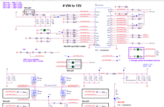
My customer finish their LM5176 circuit and start PCB design. Would you please helping to check their layout? Thanks for your kindly help.
Best regards,
Gary Teng

This thread has been locked.
If you have a related question, please click the "Ask a related question" button in the top right corner. The newly created question will be automatically linked to this question.
Tool/software:
Hi Sir,
My customer finish their LM5176 circuit and start PCB design. Would you please helping to check their layout? Thanks for your kindly help.
Best regards,
Gary Teng

Hi Gary,
thank you for supporting the LM5176.
Note: based on your request i just checked the layout but did not review the schematic.
Layout
(In below list items which should be checked again have been marked bold)
Vcc Cap close to pins
AGND and PGND connected at Thermal pad - no
Via's in Thermal pad: Thermal Pad could get more via's to better distribute power loss of the LM5176
AGND island
-> a AGND power area help to avoid disturbances injected into the AGND related components
Kelvin connection to CS/CSG sense resistor
Kelvin connection to ISNS+/- sense resistor (shorted to GND if not used)
Small current loop for HDRV1/SW1 (best if wires are on top of each other)
Small current loop for HDRV2/SW2 (this one is better)
Input caps close to MOSFET
Output caps close to MOSFET
FB divider close to LM517x
PDF link:
Additional info on layout can be found here :
(1) Four-switch buck-boost layout tip No. 1: identifying the critical parts for layout
(2) Four-switch buck-boost layout tip No. 2: optimizing hot loops in the power stage
(3) Four-switch buck-boost layout tip No. 3: separating differential sense lines from power planes
(4) Four-switch buck-boost layout tip No. 4: routing gate-drive and return paths
Best regards,
Stefan