Other Parts Discussed in Thread: PCA9306
Tool/software:
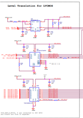
I saw the TLV7103318DSET part in the PROC141E4_RP schematic.in that I have on doubt.
This IC has two enable pin's and the EN2 is high so OUT2 comes by default (VLDO_CSI_1V8) and the 1.8V is going to all ICs connected with it.
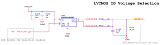
As per my understanding, if we need 3.3V, I should toggle the EN1 Pin input to high using the DIP switch and remove the R1241 resistor. Could you confirm whether this is correct?
Note:
We need the 3.3V operation for I2C and GPIO's so that I ask above clarification.