This thread has been locked.

If you have a related question, please click the "Ask a related question" button in the top right corner. The newly created question will be automatically linked to this question.

LM5160: LM5160

Part Number: LM5160

Tool/software:

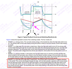
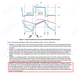
In mode3  in the figure,:t3: the primary current is negative, which can be understood, but why the current is positive  at time t0, I don't understand this switching path。

www.ti.com/.../ssztcb7.pdf

  • Hi Xiaofeng,

    Thank you for posting.  Note that Mode 3 is the really short time duration.  It is basically the dead time in which both the high side and side FETs are off, and it is a necessary internal to prevent shoot-through.

    Note that, the fly-buck circuit is still equivalent to a buck if you combine the primary and secondary circuits.  The total inductor current still satisfy the buck operation as shown in the red current curve.  In Mode 2, the total inductor current is the sum of the pri and sec currents (please note the polarity dots), and when the pri load is 0, the pri inductor current would look like the blue curve.    

    Any, at t0, only the high side FET is on, and the low side and sec diode are both off, and the total equivalent current flows the pri winding, and it is positive. 

    However, if you operate in light load running into "DCM", at t0 the pri inductor would be negative.   You may test on our EVM, or run some simulation, to get a better understanding of the phenomenon. 

    Hope this clarifies.

    Regards,

    Youhao

  • My understanding is that (as show in the arrow):during the dead time, the primary current will remain negative until the current continues to flow to 0。 and when the high-side MOS is turned on, it will be positive
  • because i can‘t find  a voltage difference that can reverse the current direction in  the dead time

  • Sorry, I deleted an inaccurate answer, and let me reply again here. 

    First, please note that the primary negative current means the current flows down into the drain of the low side FET.  Please draw out the schematic and current flow direction, if my words confuse you.  Also note that the inductor sees voltage SW-VOUT.

    During dead time, the low side FET is turned off, and its channel stops the current immediately, and the down-flowing current will charge the inherent drain-to=source capacitor to raise the SW voltage. During this process, you will see the inductor voltage, which is SW-Vout, will change, as shown in Figure 3. 

    Hope this clarifies.

    Regards,

    Youhao

  • I mean that :in the dead time (mode 3) ,why the current direction changes?from  negative to positive?

  • After the low side FET is turned off at the beginning of Mode 3,  SW voltage will rise in Mode 3 to cause the secondary diode reverse biased and to stop the secondary current, that means the reflected secondary current disappeared, and the primary current will settled to the regular buck current, which is positive in the figure.  

    I would suggest you to either monitor the signals on a circuit, or run a TINA or Pspice simulation if my answer is not clear enough.

    Thanks,

    Youhao