This thread has been locked.

If you have a related question, please click the "Ask a related question" button in the top right corner. The newly created question will be automatically linked to this question.

UCC21550: Part 2: Half bridge circuit with UCC21550 not working

Part Number: UCC21550
Other Parts Discussed in Thread: UCC27511

Tool/software:

Hi,

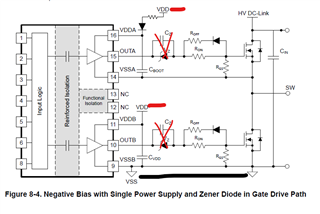
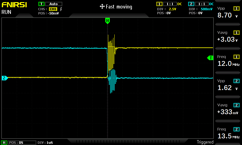
I am continuing a thread: Half bridge circuit with UCC21550 not working with Will as this thread has been locked due to inactivity for more than 30 days. 

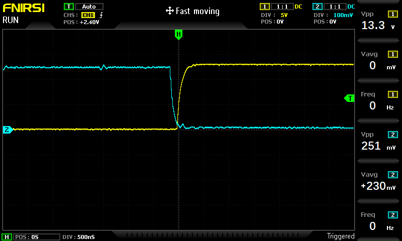
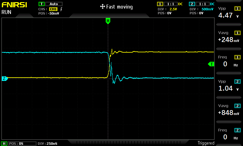
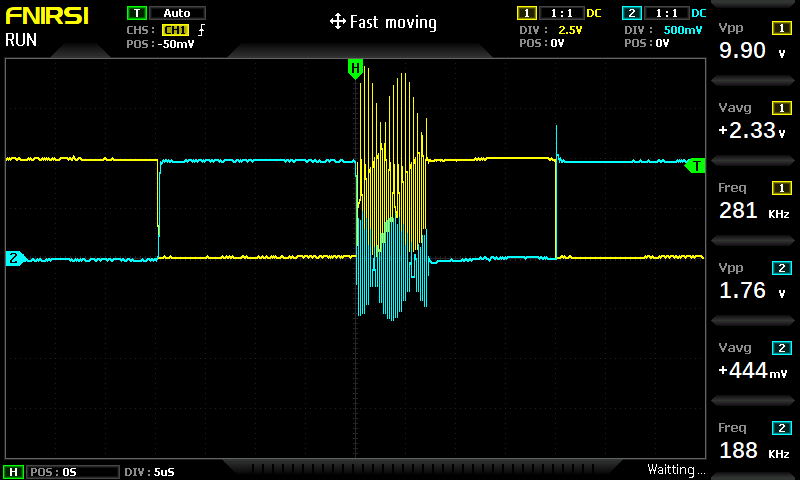
I have increased the dead time to 443ns (R_DT 50K) but the issue is not resolved. 

What else could be going on there?

Kind regards,

Bright

  • Hi, 

    I suspect the issue might be mentioned in page 31 of the UCC21550 datasheet. My configuration, does not include a zener diode to have negative ate drive bias. There is excessive ringing on the VGS. 

    Page 31

    "When parasitic inductances are introduced by non-ideal PCB layout and long package leads (for example,
    TO-220 and TO-247 type packages), there could be ringing in the gate-source drive voltage of the power
    transistor during high di/dt and dv/dt switching. If the ringing is over the threshold voltage, there is the risk of
    unintended turn-on and even shoot-through. Applying a negative bias on the gate drive is a popular way to keep
    such ringing below the threshold. Below are a few examples of implementing negative gate drive bias"

    For DC link below 46V, it switches okay, current 0.015A, power dissipation 0.4W. But the circuit design and MOSFET is intended for application DC link 400V. But once the DC link increases to  48V DC, the power dissipation goes to 20W, with temperature spike and needs to be shut down immediately.  I have attached the testing waveforms and notes in the dropbox link:

    https://www.dropbox.com/scl/fo/w42m39qjk8by2nzfwe8em/AKD_F3lE95tK83RB2KleE8w?rlkey=29rsk3qvfvg0nrhr9oocrld7j&dl=0

    The word document explain the waveform images from 1-19, and also a video that captures the transition. 

    Kind regards,

    Bright

  • Hi Bright,

    I cannot access dropbox. Can you upload and post the picture & word document here on E2E?

    It sounds like you have a lot of switch node ringing and a Miller spike that is causing shoot-through. Hopefully you have Vds and Vgs measurements so that we can confirm. The Vds ringing is caused by switch node capacitance and HV Bus inductance when the high-side switch closes. Usually I need to respin the PCB several times to line up the resonance just right so that my decoupling network can critically damp the resonant frequency. What FETs are you using? 

    Miller injection can be absorbed with a local turn-off buffer. I use UCC27511 right between the gate and source pin of the FET to buffer the low-side of my further away half-bridge gate driver. This minimizes the turn-off inductance, and helps reduce the Miller spike across Vgs.

    Also, you can add some distance between the switch node and the low-side FET. This will add a tiny amount of inductance that can help absorb dVds/dt across the low-side, which reduces the injected Miller current.

    Finally, snubbers on the HV BUS will be shorted to the switch node when it is ringing. Electrolytic capacitors can add resistance and capacitance to the rail, and can be an effective snubber for switch node ringing since they are large and can handle the thermal load.

    Best regards,

    Sean 

  • Hi Sean,

    Is the zener diode required for the negative bias? to ensure that it is fully turned off?

    Attached are the waveforms:

    The word document explain the waveform images from 1-19, and also a video that captures the transition. 

    Kind regarrds,

    Bright

                       Waveform Notes.docx

  • HI,

    Mosfet part number sihp24n80ae. VGS is 12VDD.

    Kind regards,

    Bright

  • ALso, how do you apply  UCC27511 right between the gate and source pin of the FET. Please a hand sketch diagram would be good. Thank you

  • Also,

    "Finally, snubbers on the HV BUS will be shorted to the switch node when it is ringing. Electrolytic capacitors can add resistance and capacitance to the rail, and can be an effective snubber for switch node ringing since they are large and can handle the thermal load."

    Please a sketch of the connection would be good. Thank you

  • "you can add some distance between the switch node and the low-side FET. This will add a tiny amount of inductance that can help absorb dVds/dt across the low-side, which reduces the injected Miller current."

    What is the recommended distance between the High side and low side MOSFET (T0-220 package)?

  • Hi Bright,

    The Zener diode is there to clamp the voltage charged in the capacitor Cz. The charge that is remained on Cz is the shifted voltage that creates the negative bias.

    Taking a look at the waveforms, it looks like this noise is being excited by the power stage. We have seen that some MOSFETs that are designed for high voltage applications that are extremely noisy at lower voltages. Do you have any other MOSFETs that you can try with this setup to see if that has an impact on the noise?

    The clean waveforms from the no load condition and the sudden noise increase from 44V -> 48V bus voltage makes me think it is related to the MOSFET.

    Regards,

    Hiroki

  • Hi Hiroki,

    Thank you for the response. 

    What is the recommended  value for the zener diode  and the Cz in the application?

    The application is intended for DC link 330-390, so I thought that a 800V MOSFET should be okay. Moreover, I need to test the circuit from small voltage with 5V increment until I have reached the DC link voltage. The first test that used the full DC link voltage damaged the circuit, hence, the caution to do it by stages. 

    Seeing that the application is 330-390V DC link, so what MOSFET VDS is recommended? 

    Kind regards,

    Bright

  • Also, I suspect that 800V MOSFET should work fine at low voltage.

  • Hi Bright,

    Thank you for following up.

    A 1uF capacitor should be sufficient with a ~5V Zener diode reverse voltage.

    Having a large margin for the MOSFETs is great and should not be a problem. I am not too familiar with the MOSFET being used here, but just wanted to provide some input from past experience with high voltage MOSFETs acting up at lower voltages. I recently did testing with a 650V Si MOSFET that showed very high noise from 50-300V.

    Regards,

    Hiroki

  • Hi Hiroko,

    Thank you for your response,

    But if its noisy at 50-300V, How can it be prevented/reduced to avoid shoot through before reaching the desire voltage of about 330-390V?

    Kind regards,

    Bright

  • Hi Bright,

    For my testing, I was able to completely mitigate the noise by swapping the MOSFET to a different one (SiC in my case). Most of the noise was mitigated and behaved consistently across all tested bus voltage levels 

    From other experiments, I found that increasing the gate to source capacitance with an additional capacitor helped slow down the switching and mitigate a lot of the noise. A ferrite bead on the gate of the MOSFET also helped prevent noise from entering the gate driver which can cause logic glitches if extreme enough.

    Regards,

    Hiroki

  • Also, does the zener diode in this configuration provide negative bias during turn off? or is only clamps the gate voltage?

  • Hi Hiroki,

    Thank you for the response,

    The new MOSFET that I want to used is STF28N60DM2, 600V, 130m ohms.

    1)The current gate capacitor that I have is 1000pF, is that enough? 

    2)is the ferrite bead connected after the ROFF-diode and RON resistor or before? will it not effect slow down the switching performance?

    Kind regards,

    Bright

  • 3) Also, what is the recommended value for the ferrite beads?

  • 4) Just to mention, from the previous threads,  I am using 10uF capacitive divider, midpoint connected to the load. Literally, Half bridge configuration with two MOSFETS and a capacitive divider. I hope this is not introducing additional noise to the circuit?

  • Hi Bright,

    That MOSFET looks like a good fit for your application.

    1.) Yes, that is a good value for a gate to source capacitor. The ST MOSFET has about 336nC less input capacitance so this gate to source capacitor socket will help slow down the switching if necessary to mitigate ringing.

    2.) The ferrite bead would be placed as close to the gate as possible. This ferrite bead should not have any effect on the switching performance. The impedance should only be high at the desired noise frequency range.

    Here is an application brief that goes into details about this: https://www.ti.com/lit/ab/sluaai2/sluaai2.pdf?ts=1724185330306&ref_url=https%253A%252F%252Fwww.google.com%252F 

    Refer to page 4 for the ferrite bead selection guide.

    Hope these solutions work. Please feel free to ask additional questions below!

    Regards,

    Hiroki

  • Thank you for the detailed responses.

    Does the zener diode in this configuration provide negative bias during turn off? or is only clamps the gate voltage?

    Kind regards,

    Bright

  • Also, is there any need for external diode and TVS diode across the drain source of the High and low side MOSFETS?

  • The Zener diode effectively shifts down the output signal. 

    For example if an 18V power supply is being used to power up channel A of the gate driver and a Vz = 4.7V Zener diode is used, the pull down voltage would be -4.7V and the pull up voltage would be 13.3V after several cycles in which the Cz capacitor is charged to Vz.. It is important to consider the shift down on the pull up voltage, as this value should still be above UVLO threshold after it has been shifted down.

    I believe your RC snubbers should be sufficient here. Tweaking the RC snubber values may be worth trying to help maximize the effectiveness though.

    Regards,

    Hiroki

  • Thank you. I will make the changes and inform you later on the progress.