This thread has been locked.

If you have a related question, please click the "Ask a related question" button in the top right corner. The newly created question will be automatically linked to this question.

UCC256404: Startup issue of UCC256404

Part Number: UCC256404
Other Parts Discussed in Thread: PMP40580, TL431

Tool/software:

The previous thread was locked, so I couldn't add to it, but I did realize my error with only trying to power the LLC.  I didn't think I could startup the chip with an external supply to the VDD pin - I thought it had to be charged internally through the HV pin, so that answer was helpful.

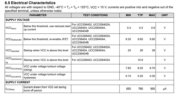
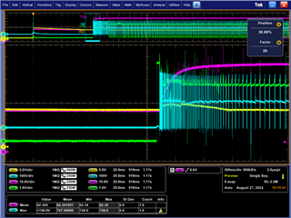
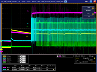
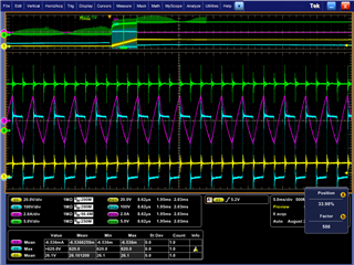
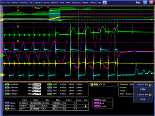
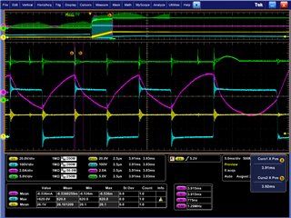
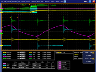
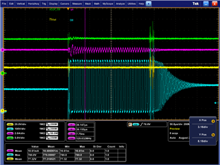
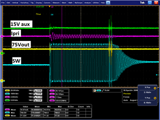
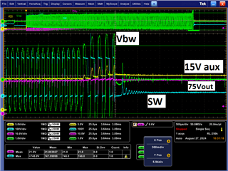
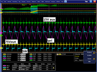
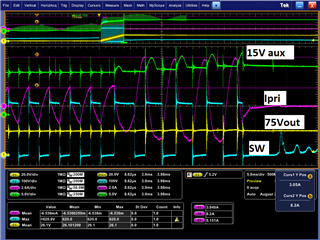
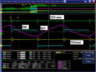
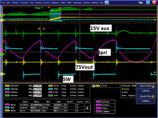
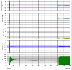
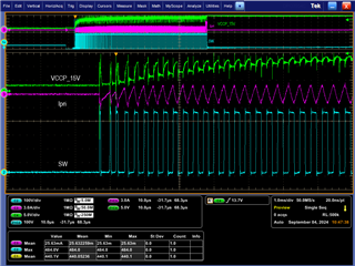
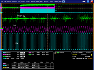
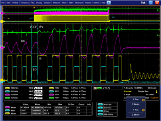
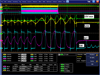
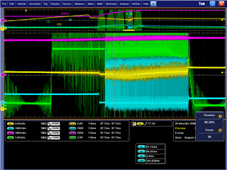
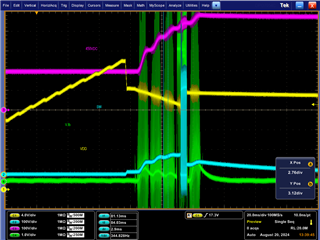
However, I'm now running into what is probably a fault on startup.  I've attached a couple scope plots, my schematic, the transformer datasheet I'm using, my excel design sheet, as well as the simplis model of my design for reference.  The good thing, I think, is that the simplis model mimics my measurements on the bench, but I'm not entirely sure where to start looking for problems.  My biggest concern is whether I've modeled the transformer properly, but I think all of the values in my design match what I get from the design spreadsheet.  The scope plots show the 450V input, the VDD pin, the FB pin, and the switching node SW.

General specs of the LLC design -

Vin is 450VDC; Vout is 75VDC; Iout max is 2.667A.

The UCC256404 starts switch, and then stops after about 5ms, which is what the sim does, too, though the sim does restart after another 30ms or so, and my PCB does not.  I attribute that to certain fault modes not being implemented.  The output of the LLC (not shown in the scope plot) should regulate to 75V, but it gets to only about 40-45V before something shuts it down, also the same as the sim.

I'd appreciate a look over my design sheet and/or schematic to see if I've done anything incorrectly, or some thoughts on where to look for issues.  I'm new to both LLC designs and SIMPLIS, so I definitely have a learning curve I'm navigating.

Thanks,
Joe

 UCC25640x Design Calculator Rev4 take2.xlsx

LLC Transformer.pdf3630.n10812F-0_Schematic_Aug5_2024.pdfUCC25640x Simulation Test Bench ERGdesign.zip

  • Hello,

    Your inquiry is under review and I will get back to you shortly.

    Regards,

  • Hello,

    It looks like your design is starting up by VCC reaching VCCstartself voltage.  Switching begins then VCC drops down to around 17 V.

    For the device to turnoff do to UVLO the output needs to drop down to below 8 V roughly.  So your design is not shutting down do to VCC not being regulated.

    The things that will cause your design to shutdown and not regulate is over current, input or output OVP.  Figuring out which one is being triggered will help you determine which fault you are seeing.

    You might want to evaluate IFB, ISNS, SS and Vout during power to see which fault is being triggered. 

    Regards,

  • Sorry - been on vacation the past week.

    If I zoom out on the scope to 500ms/div, the converter will actually startup and regulate.  It's about 1s, so that does suggest that it's the fault recovery timer.  The first couple plots below are showing that with a zoom in on the startup after the 1s delay.

    I'm using the UCC256404 chip, which I didn't think had input OVP (only the -402A variant does, right?), so I don't think it's that. 

    .

    The 75V output is not going over voltage, however, the BW pin thinks that it is.  In the plot below, the green trace is the BW pin, and the cursors are set to +/-4V.  After the required 5 cycles of being beyond 4V, a fault is declared (I assume).  The yellow trace is the primary side 15V rail.  Something during this time is causing it to be pushed up to 25V briefly.  This occurs when the SW node goes high (so the top FET of the halfbridge is on), but it only persists for about half the during that the SW node is high.  Does this suggest that my layout is suspect?  Or the transformer construction?

    When the converter catches during the second startup, I do not see these blips on the 15V rail - it regulates just fine.

    Thanks,
    Joe

  • Hello,

    Your inquiry has been received and is under review.

    Regards,

  • Hello,

    The UCC256404 does not have bulk OVP.  However it does have output OVP that is measured on the output winding.

    Do you think this might be what is shutting down your design?

    Regards,

  • Yes, I'm nearly positive that the output OVP is being tripped (though I don't know the cause).  That's what the last plot is showing.  My primary aux rail (yellow trace) shows humps during the last 5 switching cycles when the high side FET is on.  This pushes what should be about a 16V rail up to 25V, which causes the BW pin (green trace) to see voltages beyond the fault limits (green horizontal cursors).  The actual output of the converter is a 75V rail on the secondary of the transformer.  That's the purple trace.  At the time of the fault, it has only reached about 40V, so there isn't any real overvoltage there, but because the primary aux rail gets pushed up, the chip thinks there is.

    If you look at those last few switching cycles, it looks like something changes the timing of the primary FETs' gates.  It jumps from a frequency of about 175kHz to 117kHz in one cycle, and also doesn't appear like the last five cycles are at 50% duty.  I don't have a ton of experience with LLCs, but my understanding is that they are always supposed to run at 50% duty cycle (with some dead time in between FET turn-ons), but change frequency to adjust how much energy is transferred through to the secondary.  If 50% duty cycle isn't maintained, wouldn't that imbalance the energy stored in the primary of the transformer?  I could see how that would cause the blips on the aux rail, but I don't know what the root cause of the non-50% duty cycle would be.

  • Not sure if these plots will help, but figured I'd add them.  I added a wire loop to the primary of the transformer so I could take a look, and here are a few plots showing that.  These are all the same plot with different zoom point.  15V primary aux rail in green, Ipri in purple, SW in blue, and Vout in yellow.

    I did notice that when the converter catches after the first fault, and enters burst mode (I'm running this into a light load for the moment), I do still see those blips on the 15V primary aux rail for the first couple cycles, though they are greatly diminished in amplitude:

    Those blips, though, I think are a symptom rather than a cause.  They only seem to occur during transitions in switching frequency.

    Another concern is that I think I'm getting higher primary current than I'd expect during startup.  I get about 3A peak primary current in my plot, but the design excel sheet would suggest I should only get 1.357A in the primary.  I don't know if that number is expected to be exceeded during startup, but the excel sheet seems to suggest it shouldn't, as it gives a required rating of that number for the resonant inductor (cell C118).  Here's an updated design file with all the values I have on the board entered, in case it helps -

    UCC25640x Design Calculator Rev4 new Lmag of 510.xlsx

    Thanks,
    Joe

  • Hello,

    Have you checked your resistor divider to the BW pin to see if it is setup correctly?

    Also note that noise on the BW pin can also trigger and OVP.  You can add capacitance to this pin to reduce the noise.

    Regards,

  • Hello,

    Just had a chance to check the waveforms.   I am collared blind.  Could you label the waveforms and resend them?

    Regards, 

  • I'm pretty sure the BW resistors are set properly.  This isn't a trip due to switching noise, I don't think.  My primary aux rail really is getting pushed up, causing the BW pin to get pushed up.  It faults after 5 cycles, like the datasheet says.  I do have a cap at the BW pin of 10pF, which is suggested by the design excel sheet.  But this is all preceded by a change in the FET gate signals.  I just don't know what causes that - something with the soft start value?  A problem with the transformer construction (e.g. - the leakage value being incorrect)?  Does it suggest a layout issue?

    I would have done a better job of labeling the plots if I knew - sorry about that.  Here's my best try of labeling the important plots.  If need be, I can try and retake them.  There are labels on the plots, but they are the same color as the traces - not sure if that's helpful for you or not.

    During burst mode of the converter, after it catches (i.e. - running normally into a light load)

    Last few cycles before the startup fault:

    During startup, before the fault is declared.  Ipri is the triagularish waveform, SW is the square wave, in case the labels aren't clear.

    Same plot as above, but zoomed into the last few cycles before the fault is declared.  You can see the SW waveform change, and then Ipri drastically increase during the last few cycles.

    Same plot as above, but zoomed into just a couple of switching cycles before the startup fault.

    Same plot as above, but zoomed into the couple of switching cycles where the startup fault starts to happen -

  • Hello,

    When I look at the 15 V aux voltage there are 5 V jumps.  This should result in a Vaux*Ns/Na = 5V*5 = 25 V jump on your 75 V output.

    When I look at your 75 V output it looks like it is 7.5 V per sub division.  A 25 V change on the output would result in a 3.33 subdivision change. Which I am not seeing on your waveform below.

    If the 75 V is stable the output transformer and diodes should clamp the 15 V aux from gaining an additional  5 V. 

    I checked your schematic for the LLC and it looks O.K.  So I can't see that is an issue.

    You might want to double check your schematic to make sure it matches your layout.  Please note that layout review is not a service that is provided on the e2e.  However, this might be where you issue is.

    The other thing you might want to study is the voltage across your transformer to see that it behaves as you expect.  There might be something in wrong in the transformer design as well causing this issue.  So I would suggest double checking that.

    Regards, 

  • Because this is during startup, the 75V rail isn't actually 75V yet.  It's around 40V at the time of the fault.  But, you are correct that I do not see the same jumps on the 75V rail that I do on the 15V one.

    My layout does match my schematic, though I can't say for sure that there isn't a grounding issue or something like that.  I did my best to mimic the layout and routing shown in fig 9-2 on page 71 of the UCC256404's datasheet.  If looking at my layout isn't something that can be done on the e2e forums, does TI have any FAE's I could email/chat with?

    I have sent this problem over to the transformer manufacturer, but this happens on multiple parts, and the transformers' measurements match what I asked for (which matched what I get in the excel design file), so I don't think that'd be the issue.

    I did notice a couple things while looking at this, though.  Those bumps do happen early on in startup, but level out as long as the switching frequency isn't changing.  In addition, my 15V primary aux looks to charge up faster than my secondary aux, even though the primary aux has more capacitance on it.

    This does seem to be pointing towards a layout issue.

  • Also, I'm still a bit curious as to the peak current issue.  In the plots prior to the last few cycles where I get the fault, my peak primary current is about 3.5A.  When the switching frequency changes from 175kHz to 117kHz (the start of the last ~5 cycles), I get a peak primary side current of around 8.2A.  Both of those numbers seem really high.  The design file suggests that my max resonant current should only be about 1.92A, though I'm unclear whether that number applies to startup.  Even if it doesn't, however, that 8.2A number is above the OCP1 limit of 5.71A (using 150pF, 140ohm for the Isns components).  That points me away from a layout issue, I think, and more towards a component value or calculation issue.

  • Hello,

    Your questions has been received.  However do to US holiday I will not be able to look into until Tuesday.

    Regards,

  • No worries - I'm also out of the office until Tuesday.

  • I'm not sure if this is helpful, but the SIMPLIS sim file that TI has for the UCC256404 acts kind of similar to my board during startup:UCC25640x Simulation Test Bench ERGdesign Sept3.zip

    The sim has been updated to match my design with the exception of the secondary configuration.  The sim has D3 and D4 connected to gnd and the center tap of the transformer being Vout.  My design is the opposite - diodes connect to Vout and the center tap is ground.  If I change the sim to match that, the simulation time increases significantly.  I don't think the diode orientation should matter for the overall behavior of the converter, so I just left them as is.

    If you run the sim, and look at the current through the transformer, the startup current is huge.  Once the converter starts regulating, though (around 165ms in the sim), the currents are much more in line with what I expect.  The magnetizing current sits at around the correct value throughout, but the DVM_ILR measurement, which includes the leakage inductance is 10x during startup.  I'm sure some of that can be attributed to simulation weirdness like initial conditions not being precise, and the esr for some components not being correct, but that seems a huge difference.

    At ~165ms, the sim regulates to 75V on the output, and then at 175ms, I do a load step from 0.1A to 2.667A (max current for my design), and the simulation gives me pretty expected values.  I haven't been able to do that load testing on my actual board because of the converter doesn't start properly.  But, after my design catches and runs in burst mode, the primary side current seems reasonable, and is no where near the amplitude I see during startup (this is shown in the first plot I posted to has bigger labels on it, above).

    With the high peak currents during startup, my Isns pin is getting to ~6V, which is above OCP1.  After 4 cycles of that, the converter will declare a fault.  So, I'm actually not sure which fault is being declared - either BW being greater than 4V for 5 consecutive cycles or ISNS being greater than 5V for 4 consecutive cycles.  Both happen (the too-high V.Isns value also appears in the sim, though the sim doesn't have any faults modeled), but I don't know which actually causes the converter to fault.  Is there a way to prevent those huge current peaks during startup?  Since I'm using a two parts for the resonant capacitance, do I need to add balancing resistors across them?  I didn't see any in the PMP40580 reference design, so I didn't put any on my board.  

    Are there other plots that might help debug this?  I'm at a point where I'm not really sure how to proceed.  I hate just changing random things to see the effect - I'd like to understand what is actually happening.

    Thanks,
    Joe

  • Hello,

    Your inquiry is under review.

    Regards,

  • A bit more info to consider -

    I charted the switching frequency from initial switching cycles to the fault condition, along with the SS pin and FB pin.  During the entire startup until the fault, the FB pin sits higher than the SS pin by a few volts (FB is greater than 5V, and SS only gets to about 1.1V at the time of the fault), so the chip should be using only the SS pin's voltage in the control loop, correct?

    Here is the sequence that I measure -

    I turn on the AC line into the PFC boost converter, which charges up the PFC output.  Once that hits around 430V, the LLC converter begins its startup.  The SS pin charges to about 0.23V, at which point the SW node pulls low (LO side FET is turned on).  The SS pin continues to charge until about 0.28V, and then the LLC switching begins.  This happens about 265us after the SW node pulls low.  After the first few switching cycles,

    the converter is running at about 350kHz, and has a ~50% duty cycle on each of the switches.  You can see, though, the the 15V aux rail (top trace) does get those same bumps for the first few cycles.  This seems to occur when the average current in the transformer primary is not 0.  In this case, it is just because current is starting to flow and takes a few cycles to even out.  You can see the amplitude of the bumps decreases as the current becomes centered around 0.  After only a couple hundred microseconds, the bumps are no longer there -

    As startup progresses, I measure the following values -

    At 1ms from the time that SW initially pulls low, Fsw is 200kHz, and the SS pin is 0.49V.
    At 2ms, Fsw is 192kHz, and SS is 0.68V.
    At 3ms, Fsw is 180kHz, and SS is 0.85V.
    At 4ms, Fsw is 172kHz, and SS is 1.03V.
    At 4.58ms, the last "good" switching cycle, Fsw is 167kHz and SS is 1.13V.

    Throughout all of this, the duty cycle of both the LO and HI FETs is right around 50%, keeping the average current in the primary around 0.  There is also a pretty linear progression of decrease in Fsw as SS charges.  Up until this point, the converter is behaving the way I'd expect.

    The first "bad" switching cycle has the LO FET on for 4.05us, then the HI on for 6us (for an Fsw of 98kHz).  This creates the start of a non-zero current average in the primary, which makes a bump appear.  Over the last 5 cycles before the fault is declared, the LO on time drops to 3.87us, and the HI on time drops to 4.4us (Fsw of about 121kHz).  But, because the on-times aren't the same, the current in the primary gets biased away from an average of 0.

    Something causes a significant step in the timing on the LO FET's turn off between the last "good" cycle and the first "bad" cycle.  The LO on-time jumps from about 2.8us to 4.05us is a single cycle.  The HI on-time jumps from 2.8us to 6us.  These times are never identical each power-up, but the general scheme is the same:

    I'm not sure what exactly would trigger this step in Fsw.  LO is supposed to turn off when the VCR voltage is less than VTL.  You can see the the VCR voltage appears to be steady from cycle to cycle, but the LO turn off is delayed (you can see VCR dropping below its previous value during the first bad cycle)-

    This leads me to believe that the VTL threshold has changed, but that should only occur when the voltage compensator loop comes into play.  FB is still way above SS at this point (5.5V compared to 1.1V), so VTL should still be linearly decreasing, right?

    Thanks,
    Joe

  • Hello,

    Your inquiry is under review and I will get back to you shortly.

    Regards,

  • Hello,

    Please see my comments below.

    A bit more info to consider -

    I charted the switching frequency from initial switching cycles to the fault condition, along with the SS pin and FB pin.  During the entire startup until the fault, the FB pin sits higher than the SS pin by a few volts (FB is greater than 5V, and SS only gets to about 1.1V at the time of the fault), so the chip should be using only the SS pin's voltage in the control loop, correct?

    > If the SS voltage is less than FB it will control the switching frequency.   Your are correct.

    Here is the sequence that I measure -

    I turn on the AC line into the PFC boost converter, which charges up the PFC output.  Once that hits around 430V, the LLC converter begins its startup.  The SS pin charges to about 0.23V, at which point the SW node pulls low (LO side FET is turned on).  The SS pin continues to charge until about 0.28V, and then the LLC switching begins.  This happens about 265us after the SW node pulls low.  After the first few switching cycles,

    the converter is running at about 350kHz, and has a ~50% duty cycle on each of the switches.  You can see, though, the the 15V aux rail (top trace) does get those same bumps for the first few cycles.  This seems to occur when the average current in the transformer primary is not 0.  In this case, it is just because current is starting to flow and takes a few cycles to even out.  You can see the amplitude of the bumps decreases as the current becomes centered around 0.  After only a couple hundred microseconds, the bumps are no longer there -

    As startup progresses, I measure the following values -

    At 1ms from the time that SW initially pulls low, Fsw is 200kHz, and the SS pin is 0.49V.
    At 2ms, Fsw is 192kHz, and SS is 0.68V.
    At 3ms, Fsw is 180kHz, and SS is 0.85V.
    At 4ms, Fsw is 172kHz, and SS is 1.03V.
    At 4.58ms, the last "good" switching cycle, Fsw is 167kHz and SS is 1.13V.

    Throughout all of this, the duty cycle of both the LO and HI FETs is right around 50%, keeping the average current in the primary around 0.  There is also a pretty linear progression of decrease in Fsw as SS charges.  Up until this point, the converter is behaving the way I'd expect.

    The first "bad" switching cycle has the LO FET on for 4.05us, then the HI on for 6us (for an Fsw of 98kHz).  This creates the start of a non-zero current average in the primary, which makes a bump appear.  Over the last 5 cycles before the fault is declared, the LO on time drops to 3.87us, and the HI on time drops to 4.4us (Fsw of about 121kHz).  But, because the on-times aren't the same, the current in the primary gets biased away from an average of 0.

    Something causes a significant step in the timing on the LO FET's turn off between the last "good" cycle and the first "bad" cycle.  The LO on-time jumps from about 2.8us to 4.05us is a single cycle.  The HI on-time jumps from 2.8us to 6us.  These times are never identical each power-up, but the general scheme is the same:

    I'm not sure what exactly would trigger this step in Fsw.  LO is supposed to turn off when the VCR voltage is less than VTL.  You can see the the VCR voltage appears to be steady from cycle to cycle, but the LO turn off is delayed (you can see VCR dropping below its previous value during the first bad cycle)-

    This leads me to believe that the VTL threshold has changed, but that should only occur when the voltage compensator loop comes into play.  FB is still way above SS at this point (5.5V compared to 1.1V), so VTL should still be linearly decreasing, right?

    >If the peak and of VCR and frequency change this should be due the internal FBreplica current that is controlled by the FB current.

    >So you are correct that the FB current is demanding this lower frequency triggering the OVP.

    >I double checked your schematic and see that you are using a TL431 in the feedback.  I believe this device needs 1 mA of bias current to operate correctly.

    >I wonder if the lack of this bias current is causing your issue.  Try putting a 680 ohm resistor across the opto diode (IS01) to see if the issue goes away.

    Regards,

  • This looks like it worked.  I still want to run more tests, but startup looks much cleaner with a 1k R across the opto's diode (didn't have a 680 ohm handy).  I confess to not quite understanding why, though.  I wasn't really focusing on the FB loop because it shouldn't have even been in play, yet.  With Vout only being at 40V when the fault happened, I assumed the TL431 wouldn't be contributing to anything, yet.  But, with the 1k there, the spikes on the 15V rail go away, the current waveform is much cleaner, and there is no abrupt change in switching frequency.

    I am regulating a bit higher than I'd expect, though, at least in burst mode.  My divider into the TL431 should put me at about 77.5V, but I'm bursting between 88V and 91V.  However, at least the converter in operating enough for me to start looking into that.  Thanks for the help.

  • Hello,

    The UCC256404 controls the switching frequency with variations in the FB pin current.  Which is varied from 0 to 82 uA roughly.  Not sure what the CTR is of your opto but all the currents are below the 1 mA needed to bias the TL431.

    Since this recommend solved your issue.  Could you please hit solved on the thread.

    Regards,

  • So unfortunately, this did not resolve my issue like I thought (Not sure if I'm supposed to continue this thread or ask a new question since I already marked this as resolved).  It just masked it with another issue.  Putting a 1k R across the opto's diode just prevented any current from flowing through the opto, so FB just got pegged high.  What I thought was happening was that it was hitting regulation, and then going into burst mode (albeit a little higher than I wanted), but what was actually happening is that it was hitting the OVP limit, and continually hiccupping at 1s.  I lowered the series R of the opto (R67) from 15k to 6.98k, which did allow current to flow through the opto, which put me back to very similar waveforms I've been seeing with the jump in Fsw and bumps on my 15V primary rail.  Removing the 1k R across the diode after changing the series R to 6.98k did nothing.

    I do think this points to something with the FB signal, though.  With the 1k in there, the converter was running with 0 feedback, as if the opto wasn't even present.  In that case, the softstart looked quite smooth (until the OVP fault was declared).  I only see the Lo/HI imbalance or abrupt Fsw change when the FB pin has activity on it.

  • Hello,

    You putting a 1 k resistor should just ensure the opto has bias current.  I did recommend using 680 ohms to ensure 1 mA of current.  A 1 k ohm resistor would guarantee 600 uA of bias current to the TL431.     You need to decrease the 1 k ohm to ensure there is at least 1 mA of bias current.

    If the output is above regulation there should be no opto diode current.   So this might be accurate.  Also this would go along with your design hitting OVP.

    So at light load the design is going to burst.  However, it should not hit OVP.  You might consider adding more output capacitance and/or pre-load on the output to prevent OVP.

    Regards,