This thread has been locked.

If you have a related question, please click the "Ask a related question" button in the top right corner. The newly created question will be automatically linked to this question.

LM5026: Efficiency and PMOS issue

Part Number: LM5026
Other Parts Discussed in Thread: PMP11478, PMP22075,

Tool/software:

Hi Sir,

customer refer the RT and TIME pin resistance value in the PMP11478 schematic, but efficiency is not good(only 58~60%) under the condition( 20v vin to 57v/2A output), and also the clamp p-ch MOS will heat.

but after we refer to the resstance value of RT and TIME pin in the PMP22075 circuit ,  the efficiency improve to 80%, and clamp P-ch MOS temperature dropped.

how to calculate RT and Time pin? is there Excel tool  for LM5026?

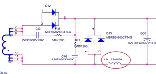
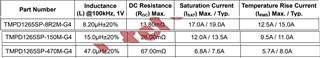
the attached is schematic and transformer/ N-MOS/ P-MOS specification as below, and we specification is vin=20~57v / vout=57v/ 2A condition.

IPGS-2504AP-LM5026.pdf

AE2214-BE_SPEC REV01.pdf

Cystek-MTEF1P15AV8.pdf

Cystek-MTE6D5N12RH8.pdf

  • TI has many resources available for designing an active clamp forward converter. Also, consider more resources available in the UCC2897A product folder and for designing/understanding the power stage take a look at Application Report SLUA535A. Optimizing the controller behavior to the characteristics of the power stage is critical for achieving high efficiency and high performance. Although you were able to increase the efficiency from 58% to 80%, this is still quite low for what is achievable with this topology. For your power stage and input/output conditions determine:

    1. Max steady state duty cycle you expect, then consider transient conditions and set the max duty cycle clamp accordingly
    2. The amount of dead time (or overlap) time required. LM5026 is unique because it allow dead time (high-side, N-channel clamp) or overlap (low-side, P-channel clamp) to be set through the RSET pin as described in section 7.3.3 of the data sheet.

    Also, consider to download and try TI Power Stage Designer - I believe there is a model for active clamp forward.

    Regards,

    Steve

  • Hi Steve,

    How to calculate L6 of the schematic in attachment? it does not  seem to be mentioned in the datasheet.

  • L6 is the output inductor that form part of a two-pole LC filter. You select this inductor based on the amount of allowable ripple current the inductor will see. Typical is IL=0.2*Iout_max. The trade off is if you allow more ripple current, the inductor will be smaller but the RMS current into the output capacitor(s) will be larger. If you allow less ripple current, the inductor will be larger, higher DC loss (Iout_max^2*RDC).

    L=V*(Δt/ΔI), where:

    ΔI=IL

    Δt=ton

    V=Von

    Regards,

    Steve

  • Hi Steve,

    thanks for your information, you mean  i can calculate it as below:

    Fw=200k = 1/T = 1/ 200K= 5u/S

    ΔI=IL = 0.2 * 2.5A = 0.5A

    L= 56v * ( 5u/ 0.5A)= 560uH.. 

    is our calculation correct? it seems wrong~

    and also we try to modify L6 from 8.2uH ~47uH, we get the follwing result:: 

    1. 8.2u==> Vin 47v above / output 56v, full loading 2.5A==>pass.

                      but input is below 47v/ the output 56v, it can not be full loading 2.5A==> fail.

    2. 47u==> vin 46v above / output 56v, can not full loading 2.5A==>fail

                      but  vin below 46v/ full loading 2.5A can be pass.

    3. 15u==final test result of the 15uH inductor, input can be from 20v~56v, the output is 56v/full loading 2.5A, total 140 watt, verification pass.

      we want to know if use L6_15uH inductor have any risk? can this value be used? 

    sorry~let us learn from you, and looking forward to you reply, thanks.

  • You need to use ton and Von instead of T and VIN.

    Steve

  • Hi Steve,

    could help give us some comment and suggeation below? thanks.

    and also we try to modify L6 from 8.2uH ~47uH, we get the follwing result:: 

    1. 8.2u==> Vin 47v above / output 56v, full loading 2.5A==>pass.

                      but input is below 47v/ the output 56v, it can not be full loading 2.5A==> fail.

    2. 47u==> vin 46v above / output 56v, can not full loading 2.5A==>fail

                      but  vin below 46v/ full loading 2.5A can be pass.

    3. 15u==final test result of the 15uH inductor, input can be from 20v~56v, the output is 56v/full loading 2.5A, total 140 watt, verification pass.

      we want to know if use L6_15uH inductor have any risk? can this value be used? 

    sorry~let us learn from you, and looking forward to you reply, thanks.

  • Lower inductor value, increased peak-to-peak ripple current, the inductor will be smaller but the RMS current into the output capacitor(s) will be larger. Larger inductor value, decreased peak-to-peak ripple current, the inductor will be larger, higher DC loss (Iout_max^2*RDC).

    Instead of guessing an inductor value that seems to allow the output to regulate over the full range, you need to figure output why it's not regulating under some conditions. I recommend to investigate the feedback, opto bias and current sense signals to make sure they are within the range you expect where the output should be regulating.

    Steve

  • Hi Steve,

    got it , thanks.