This thread has been locked.

If you have a related question, please click the "Ask a related question" button in the top right corner. The newly created question will be automatically linked to this question.

LM5146: Switching frequency issue

Part Number: LM5146

Tool/software:

Hi TI experts,

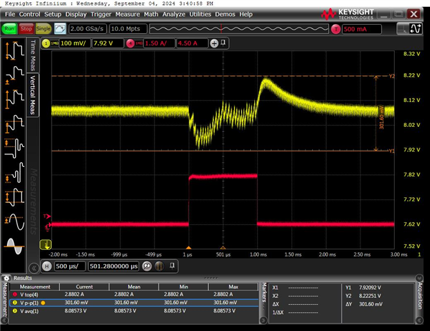
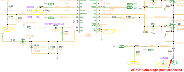
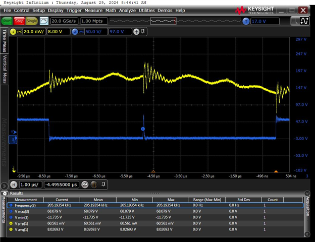
I use LM5146 to convert 54V to 8V/13A, the Fsw was set to 200kHz by connecting 49.9Kohm to RT pin.

Observed one pulse in every two is missing and duty cycle is incorrect.

Can you help look into this issue?
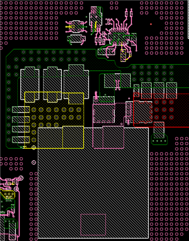
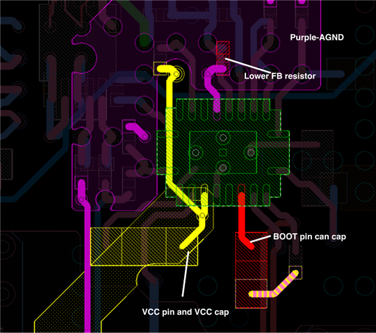
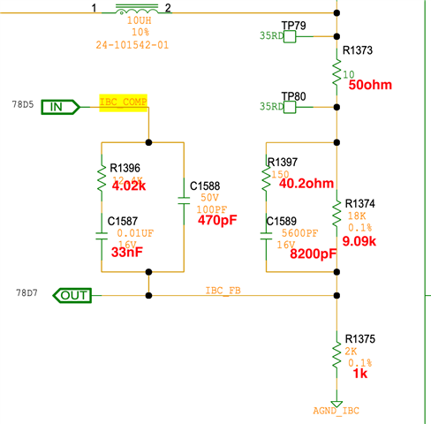
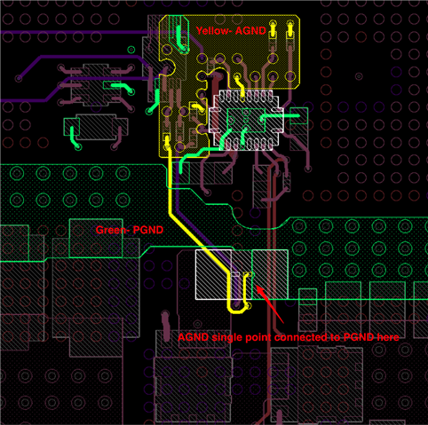
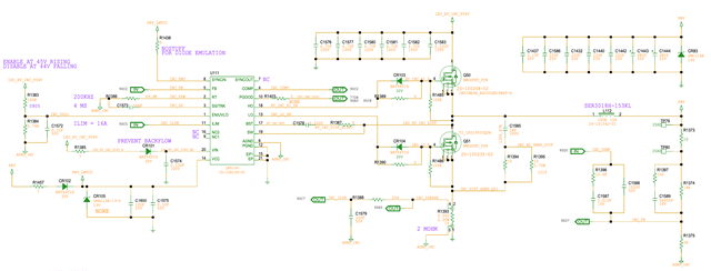
Schematic:

Yellow- Vout, Blue- Switching node

Yellow- Vout, Blue- Switching node, zoom in

Thanks

Neo

  • Hi Neo,

    I suspect the design is unstable - please complete the quickstart calculator to check https://www.ti.com/tool/LM5145DESIGN-CALC. Note the 22uF/25V output cap will be ~10uF at 8VDC. Set the crossover < 25kHz. what is the ESR of the electrolytic?

    We may also want to review the layout. Please refer to the layout guidelines in the data sheet and see app note SNVA803 for input cap placement.

    Regards,

    Tim

  • Hi Timothy,

    Attached the calculator. The loop parameters look good. Please help check.

    LM5146-Q1 Quickstart Tool r2 - 55Vin 8Vout 12p5A 200kHz_FET_updated_Bottom_FET_CSD19533Q5A_10uH inductor.xlsm
    Thanks

    Neo

  • Here is total output capacitance for this design for re-check the loop compensation.
    100uFx2 Poscap, ESR=55mohm
    68uFx4 Poscap, ESR=70mohm

    22uFx28 MLCC, ESR=4mohm

    10uFx8 MLCC, ESR=8mohm

    Below the snap shot for layout. Do you need layout file for review?
    Red-Input, Yellow-Output, Green-GND.

    Here is the bode plot we captured.

    3A loading:

    8A loading:

  • Here are some comments:

    1. The low-side FET has very high Qrr, possibly causing some noise, and is quite capacitive. Try using the same FET as the high side, and remove the diode and gate resistor on the low-side FET.
    2. Snubber cap at 1nF is high.
    3. The shunt is a bit low at 2mΩ. Better to use Rdson current sensing.
    4. CR102 needs to be a Schottky to have any chance of pulling VCC above its nominal 7.5V and thus derive bias power from Vout.
    5. Make sure the VCC and BOOT caps are close to their respective pins.
    6. Check that the lower feedback resistor is close to FB and AGND pins.
    7. Try to get cleaner bode plot measurements. The gain is running along 0dB at 3A (it should not be that different than 8A).

    Regards,

    Tim

  • Hi Timothy,

    We did a few experiments per your suggestion.

    1. Low side diode CR104 removed, no help. Low side FET can't be same as high side due to high Rds(on). Looking for alternative FET with lower Qrr.

    2. Snubber cap removed, no help.

    3. Will shunt resistance impact the compensation loop?

    4. VCC voltage is ~7.6V. Even if lt's lower than 7.5V, the internal VCC generator will take control and this has no impact to the control loop, right?

    5. Confirmed VCC and BOOT cap are very close to respective pin.

    6. Confirmed lower FB resistor is close to FB and AGND.

    I tried to tune loop parameters, when increase C1588 to 330pF, the switching node got changed to have two normal pulses plus one abnormal pulse. Previously with C1588=100pF, there was one normal pulse plus one abnormal pulse. 

    Please provide your comments.

    C1588-=100pF

    C1588=330p

    Thanks

    Neo

  • Thanks, Neo.

    Some of the above recommendations were general circuit improvements (not related to this issue). The VCC and BOOT caps look large here. You should use 0603 size for these and place them the same as what's shown on the EVM. Also check the RT resistor placement that it's close to the RT pin.

    Here is a file that checks the effective Cout and ESR with two cap chemistries...it's important to get the effective Cout and ESR to model the compensation in the quickstart. Increasing the cap you mentioned from 100pF to 330pF reduces the pole frequency. 

    Parallel Capacitors Zct LM5145.xls

    Regards,

    Tim

  • Hi Tim,

    The effective Cout=406uF and ESR=0.31mohm per the excel calculator. I tried to adjust the loop parameters based on effective Cout and ESR, but i still saw abnormal SW pulses and random pulses got lost as waveforms i shared before.

    As for bode plot, looks like LM5146 is very sensitive to AC injection amplitude when measuring the bode plot. I changed ripple injection resistor from 10ohm to 50ohm and use adjustable AC amplitude, i can see a much clear bode plot from 100Hz to 100kHz. After 100Khz, even the amplitude is minimized to 1.25mV (FRA is AP300), i can still see rinings on bode plot, and the output ripple became unstable as shown below. Please advise for next step.

    Bode plot with adjustable AC amplitude.


    Output voltage unstable after 100Khz AC sweeping.

    Here is the updated calculator and the BOMs during debug.

    Also, for LM5146 with Rsense resistor, will the current sense participate into the loop compensation?

    LM5146-Q1 Quickstart Tool r2 - 55Vin 8Vout 12p5A 200kHz_FET_updated_Bottom_FET_BSC070N10NS3_10uH inductor_loop_tuned_ultra_debug.xlsm

    Thanks

    Neo

  • Neo,

    How does the load transient look?

    Can you use the latest version of the quickstart file online and place the high-frequency pole at Fsw/2 (using the cap from COMP to FB). This attenuates any high-frequency noise. Also, make sure the SS cap and RT resistor are close to their respective pins with short GND return.

    Regards,

    Tim

  • Hi Tim,

    I set the high frequency pole even at lower at ~50Khz per calculation, and tuned the loop.

    For light load the output ripple and bode plot looks ok, but with >9A loading, the bode plot looks uncontrollable and high oscillation can be observed on output ripple at steady state. For all conditions, the pulse is incorrect with one pulse missing in every 2 or 3 cycles.

    Please advise next step.

    Here is the waveforms.

    Bode at 7A loading.

    Bode at 9A loading.

    0-3A load step:

    8-11A load step:

    SW at 7A loading:

    Thanks

    Neo

  • Attached the latest version calculator.

    From effective capacitance calculator tool you shared earlier, effective Cout is ~400uF for my design.  But per the bode plot at light-middle loading conditions, the LC double pole is close to 2kHz, which means the effective capacitance is around 600uF. Not sure which one is correct. Please help check.

    For ILIM, does it participate into loop control? If not, can i try to disable the ILIM by leave ILIM pin floating?

    Please advise how to proceed. Thanks.

    LM(2)5145, LM5146 contorller design tool - revA1_modified.xlsm

    Thanks

    Neo

  • Hi Neo,

    ILIM is purely for current limit and does not affect the loop. There should be a resistor from SW to ILIM as shown in the datasheet - ILIM should not be left open, as it is the input to the current limit comparator.

    the other contributing factor to the LC double pole frequency is the inductance, so check if the effective value decreases with load.

    Regards,

    Tim

  • Hi Tim,

    For AGND connection, in my design AGND is single point shorted to PGND at the RLIM pin.

    Here below is the schematic and layout. Do you see any concern?


    And also, datasheet requires VCC cap to be connected to AGND, as VCC drives MOSFET which is noisy, shall the VCC cap be connected to AGND?

    Thanks

    Neo