This thread has been locked.
If you have a related question, please click the "Ask a related question" button in the top right corner. The newly created question will be automatically linked to this question.
Tool/software:
Hi,
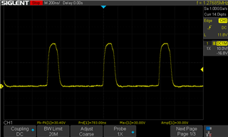
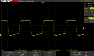
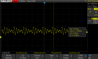
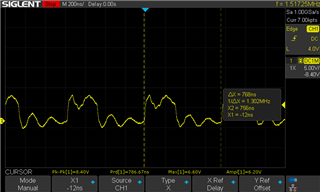
I'm using LMG1210 as half bridge driver in one of my applications in which I want switching frequency is between 1-1.5MHz. For cost saving I'm using AOD2544 MOSFET instead of using GaN FET. In half bridge configuration as provided in the LMG1210EVM-012 board, the MOSFET switching losses are very high. For average load current of approx. 1.5A with 100V as VCC, each MOSFET dissipates approx. 5W of power as per the Spice simulation and also in real life. To minimize the miller plateau effect, I've come up adding 10+10 ohm power resistors between high side and low side MOSFETs. Now the MOSFET's power loss is minimized to approx. 400mW on same load. Ignore the power loss in power resistors because that power resistors are necessary part of my load circuit.
My question is, can I design circuit like this? (Refer shared schematic). The circuit is working fine. But as the 5W resistors were heating more, I replaced them with 10R 50W aluminum casing resistors (just for testing). Power loss isn't concern, heating is. The resistors are very large in volume, so I placed them with the help of 10cm wire pieces with the board. By doing so, my LMG1210 IC blown up. I rechecked everything with onboard 5W resistors and again replaced 5W resistor with 50W big resistors and again LMG1210 IC blown up. Is there any specific reason? With that power resistors I didn't even go with 100V capacity. I increased voltage only up to 20-30V. But IC stopped giving proper outputs. And both the time, the low side switching was functioning properly, only high side driving section was damaged.
Hey Harsh,
Thanks for reaching out!
Using the 10cm wire will be causing unwanted inductance, leading to transient spikes that are harming the driver. Layout is extremely important with this GaN driver and this wire sacrifices that. Also, if you refer to Figure 3 on AOD2544 datasheet, you'll see that operating the at 5V is enough to turn the FET on but leads to greater RDSon than operating at 12V for instance.
Having the resistors in the boot charging circuit is slowing the path down and the bootstrap capacitor doesn't get fully charged. Please refer to this app note on bootstrap circuitry.
Would you please provide a scope captures of the following? (zoomed in to see one period)
Thank you,
Grant Wilson
Hi Grant Wilson,
Thanks for clarifying possible issue. The "this app note" page isn't available. Can you please share it again. And also, if you have MOSFET selection guide for high frequency switching in half-bridge, please also share that. I want to also study deeply on the effects of MOSFET input, output, reverse transfer capacitances and gate charge etc. For next version of PCB, I'm thinking about removing the power resistors from H-bridge and selecting EPC2207 MOSFET. Please also comment, whether I've chosen right MOSFET this time or not. My application requires Vds up to 130V with approx. 1.3MHz switching frequency of half-bridge. Also, please tell me whether I require a snubber circuit or not for MOSFETs?
Check out the scope captures for analysis.
Thanks
1. HO-GND
2. HS-GND
3. OUT_L-GND
4. HB-HS
5. HO-HS
Hey Harsh,
My apologies for the inactive link! You can find the mentioned app note here: ti.com/lit/an/slua887a/slua887a.pdf?ts=1726860790244
We do not have a MOSFET selection guide, but very generally the lower gate charge means the faster the FET can switch. We do have this app note you can study that discusses many of the fundamentals: Fundamentals of MOSFET and IGBT Gate Driver Circuits (Replaces SLUP169) (Rev. A) (ti.com)
Switching to a GanFET like EPC2207 will likely improve this design. As of right now, we think the power resistors could be the root of your issues. It could be beneficial to add a snubber circuit to see if this will reduce the noise.
Would you provide a combined scope capture where these waveforms are all on one plot? This will help us understand how everything lines up and hopefully help us diagnose the issue.
Best,
Grant
Thanks Grant, this resolves my issue. I don't have isolated oscilloscope probe to measure volatge w.r.t to GND at the same time measuring voltage w.r.t HS.