- Ask a related questionWhat is a related question?A related question is a question created from another question. When the related question is created, it will be automatically linked to the original question.
Tool/software:
Hi TIer
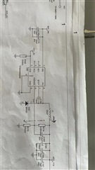
Customer use our TPS5430DDAR like this schematic.
Output is 9V (250mA - 450mA)
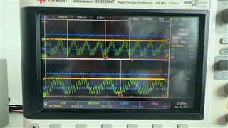
The customer will get some abnormal SW waveform similar to DCM mode in a normal SW waveform with a switching frequency of 80Khz as follows:
In the image is SW, voltage ripple and inductive current.
I think the output current is very small, so it is not overcurrent DCM protection, if it is light load DCM mode then the SW frequency should be constant.
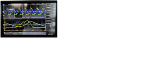
So it looks like the system is unstable and I have advised the customer to remove the C164 (type 2 compensation network) as this introduces an extra zero point.
As a result, the peak of the inductive current becomes larger, as the figure still looks abnormal, please give some comments.