This thread has been locked.

If you have a related question, please click the "Ask a related question" button in the top right corner. The newly created question will be automatically linked to this question.

TPS92692-Q1: Current ripple and DCM boundary problem

Part Number: TPS92692-Q1

Tool/software:

Hi team,

My customers are trying to design with TPS92692-Q1 for a Buck-Boost circuit with 8-16Vin and 27Vout and 105W (max 3.9A). Also, they are expecting to have a very small current ripple smaller than 200mA on Inductor and LED loads. 

In this case, I did some simple calculation and found that under 504kHz Fsw customers have to use a very big inductor around 80uH. In this case the boundary power of CCM-DCM will down to 1-2W, which is very small comparing with the 100W max power. Hence could you pls help on the questions and concerns:

1. Would this extreme small boundary power between CCM-DCM have risks/impacts on the design and some LED dimming work case?

2. Any other methods to help reduce the current ripple? Other topology that suitable for such requirements of customers?

BR,

Manu

  • Hi team,

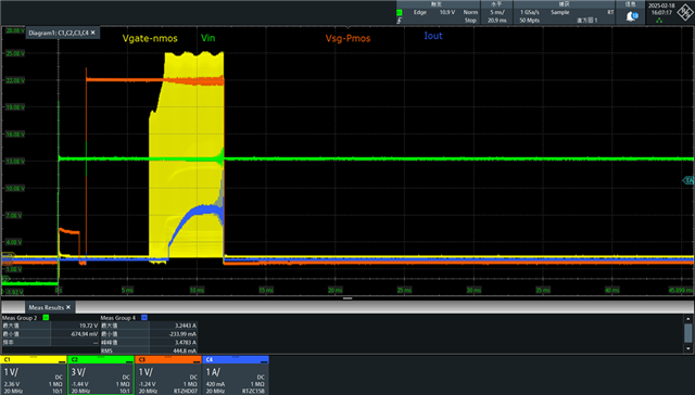
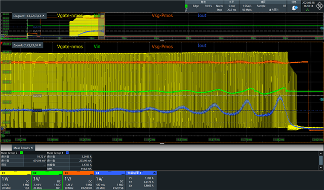
    Another app problem when customers tried use TPS92692-Q1 EVM to achieve buck-boost, they have adjusted the external components parameters as inputs in the calculator file of attachments. (Some parameters slightly different as recommended in excel: Vin=13.5V,Vout=27V,  IADJ=1V,Ccomp=15nF(no other parallel capacitors), Tsl=510K, L=25uh,Rcs=0.04Ω;Ris=0.013Ω).

    They found that when Iadj voltage is around 1V, the output is unstable and they have caught the waveform of PFET/NFET/Vin/Iout as in below figure. It seemed that some protection is triggered while the NFET and PFET are turned off. However, when customers declining the slope resistance to 220kohm and increase the Ccomp to 182nF the device can work normally.

    Pls give some suggestions on what could possible cause this and if it is recommended to adjust the slope resistors and compensation capacitors, because it seemed far away from the recommended value, thanks.

    6012.TPS92692_BuckBoost_Design_Calculator.xlsx

  • Hi Manu, I apologize for the delay as yesterday was an American national holiday. I will review your post ASAP and get back to you as soon as I am able.

    Best,
    Daniel 

  • Hi Manu,

    I am starting to review your post today

    Best,
    Daniel

  • Hi Manu,

    I have a bunch of questions.... It might be best to arrange a meeting.

    I will need you to send me the schematic so I can make sure there aren't any problems with this design.

    Why is your customer using a buck boost instead of a boost if the output voltage is always higher than the input voltage?

    What is the end application?

     Also, at low line (8Vin) you are sending a ton of current through your circuit.... assuming 90% efficiency (which is generous given expected losses due to the large current), you're probably looking at around 15 Amps at the input. This is my first concern, our device is only rated to 125 °C and I don't know what environment your customer expects this device to operate in, but you can expect the PCB to get extremely hot purely due to that power dissipation. Your customer will have to do a very good job at optimizing thermals in order to prevent our device from failing and they will likely have to use very large FETs to accommodate the power specifications. The issue with using large FETs is that the FET driver in our device is not made to drive large FETs so your customer will likely have to use an external FET driver.  We do not recommend operating our device under these conditions because I believe this will be very hard to achieve without failure. 

    Regarding the CCM-DCM boundary condition, are you saying that given the 80uF inductor, you will be in CCM above 2W out of 105W? If this is the case, that is a great margin.

    Onto your second issue... Based on the wave forms you provided, I think you will have to adjust your compensation network as this looks like some sort of instability which may be  the cause of the oscillations you see. I really need the schematic to give you more thorough feedback, but make sure your bandwidth for your compensation network isn't too wide or else the circuit will take too long to respond and will oscillate. I also want to see if any faults are being triggered which will help me figure out why your device is turning off.

    Finally, you provided values, but I don't know what "Tsl=510K" means.

    I apologize for the delays, I have been very backed up with E2E posts.

    Best,
    Daniel

  • Hi Daniel,

    Thanks for your reply. I have emailed you and let us have a meeting online to discuss this case in details.

    BR,

    Manu