Other Parts Discussed in Thread: MSP430F5529, TPS92633-Q1
Tool/software:
Greetings,
Can we connect 2 ICs of 6 PWM pins parallelly connect to a single GPIO pin of MSP430F5529?
will it work as expected ?
Best regards,
Tex
Original question:

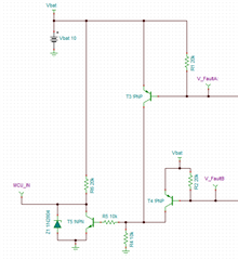
TPS92633Q1EVM: understanding of Input power supply to TPS92633-Q1
Tool/software:
Greetings,
Can we connect 2 ICs of 6 PWM pins parallelly connect to a single GPIO pin of MSP430F5529?
will it work as expected ?
Best regards,
Tex